RL78/G1H CHAPTER 31 ELECTRICAL SPECIFICATIONS
R01UH0575EJ0120 Rev. 1.20 Page 877 of 920
Dec 22, 2016
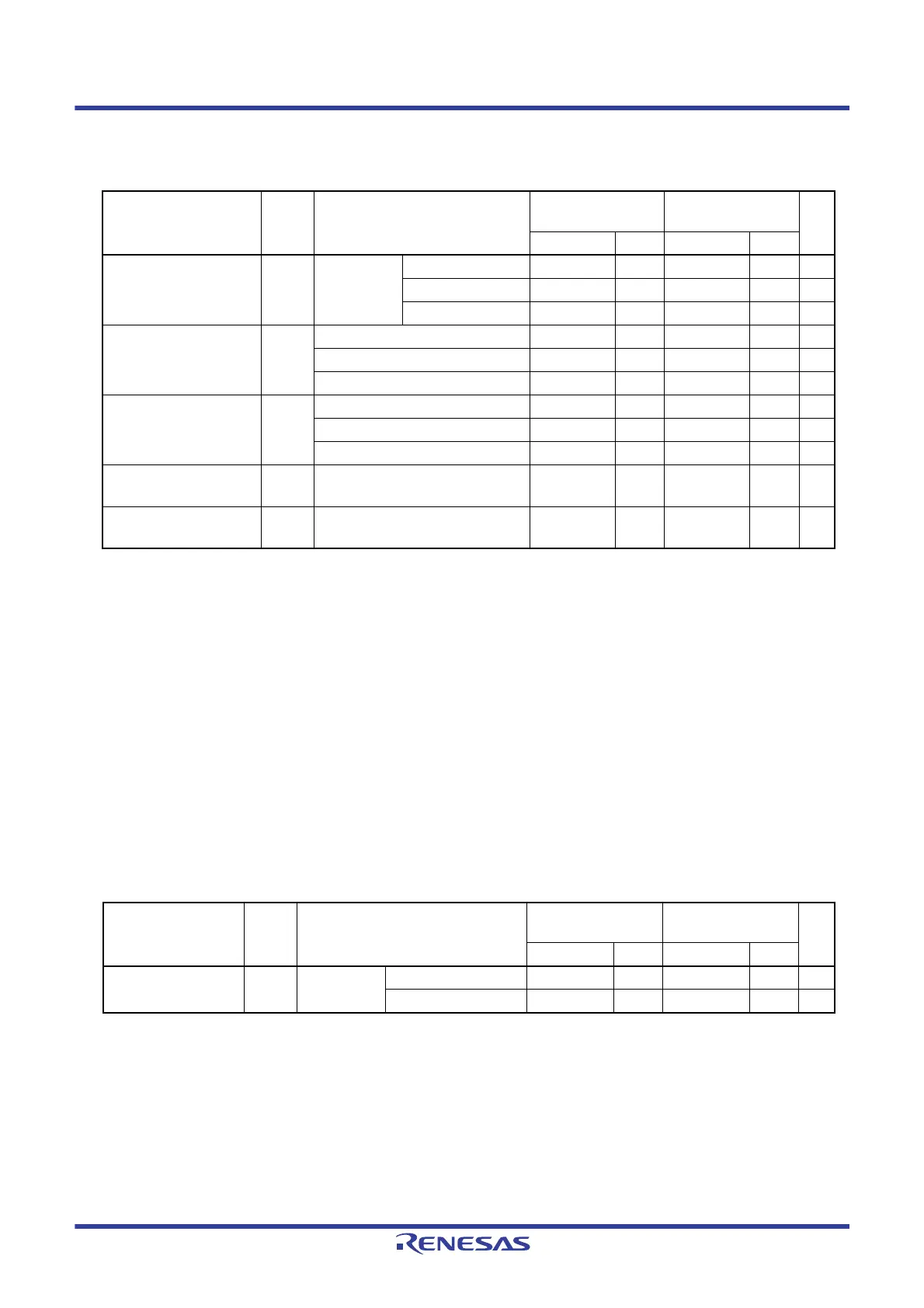
Note 1. When DAPmn = 0 and CKPmn = 0, or DAPmn = 1 and CKPmn = 1. The SIp setup time becomes “to SCKp↓” when
DAPmn = 0 and CKPmn = 1, or DAPmn = 1 and CKPmn = 0.
Note 2. When DAPmn = 0 and CKPmn = 0, or DAPmn = 1 and CKPmn = 1. The SIp hold time becomes “from SCKp↓” when
DAPmn = 0 and CKPmn = 1, or DAPmn = 1 and CKPmn = 0.
Note 3. When DAPmn = 0 and CKPmn = 0, or DAPmn = 1 and CKPmn = 1. The delay time to SOp output becomes “from
SCKp↑” when DAPmn = 0 and CKPmn = 1, or DAPmn = 1 and CKPmn = 0.
Note 4. C is the load capacitance of the SCKp and SOp output lines.
Caution Select the normal input buffer for the SIp pin and the normal output mode for the SOp pin and SCKp pin by using
port input mode register g (PIMg) and port output mode register g (POMg).
Remark
p: CSI number (p = 10, 21, 30), m: Unit number (m = 0, 1), n: Channel number (n = 1, 2),
g: PIM and POM number (g = 0, 14)
Remark p: CSI number (p = 20)
(2) During communication at same potential (CSI mode) (master mode, SCKp... internal clock output)
(T
A = ‒40 to +85 °C, 1.8 V ≤ VDD ≤ 3.6 V, VSS = 0 V)
Parameter Symbol Conditions HS (high-speed main)
mode
LS (low-speed main)
mode
Unit
MIN. MAX. MIN. MAX.
SCKp cycle time t
KCY1 tKCY1 ≥ 4/fCLK 2.7 V ≤ VDD ≤ 3.6 V 125 500 ns
2.4 V
≤ VDD ≤ 3.6 V 250 500 ns
1.8 V
≤ VDD ≤ 3.6 V 500 500 ns
SCKp high-/low-level width t
KH1,
t
KL1
2.7 V ≤ VDD ≤ 3.6 V tKCY1/2 ‒ 18 tKCY1/2 ‒ 50 ns
2.4 V
≤ VDD ≤ 3.6 V tKCY1/2 ‒ 38 tKCY1/2 ‒ 50 ns
1.8 V
≤ VDD ≤ 3.6 V tKCY1/2 ‒ 50 tKCY1/2 ‒ 50 ns
SIp setup time
(to SCKp↑)
Note 1
tSIK1 2.7 V ≤ VDD ≤ 3.6 V 44 110 ns
2.4 V
≤ VDD ≤ 3.6 V 75 110 ns
1.8 V
≤ VDD ≤ 3.6 V 110 110 ns
SIp hold time
(from SCKp↑)
Note 2
tKSI1 1.8 V ≤ VDD ≤ 3.6 V 19 19 ns
Delay time from SCKp↓ to
SOp output
Note 3
tKSO1 1.8 V ≤ VDD ≤ 3.6 V
C = 30 pF
Note 4
25 25 ns
(3) During communication at same potential (CSI mode) (master mode, SCKp... internal clock output,
supported only for CSI20)
(T
A = -40 to +85 °C, 1.8 V ≤ VDD ≤ 3.6 V, VSS = 0 V)
Parameter Symbol Conditions HS (high-speed main)
mode
LS (low-speed main)
mode
Unit
MIN. MAX. MIN. MAX.
SCKp cycle time t
KCY1 tKCY1 ≥ 4/fCLK 2.4 V ≤ VDD ≤ 3.6 V 250 500 ns
1.8 V
≤ VDD ≤ 3.6 V 500 500 ns
 Loading...


