RL78/G1H CHAPTER 31 ELECTRICAL SPECIFICATIONS
R01UH0575EJ0120 Rev. 1.20 Page 882 of 920
Dec 22, 2016
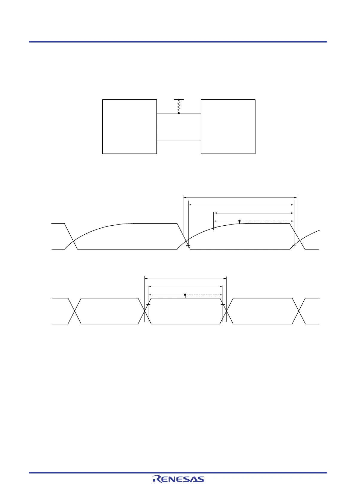
Caution Select the TTL input buffer for the RxDq pin and the N-ch open drain output (VDD tolerance) mode for the TxDq
pin by using port input mode register g (PIMg) and port output mode register g (POMg). For V
IH and VIL, see the
DC characteristics with TTL input buffer selected.
UART mode connection diagram (during communication at different potential)
UART mode bit width (during communication at different potential) (reference)
Remark 1. Rb[Ω]: Communication line (TxDq) pull-up resistance, Cb[F]: Communication line (TxDq) load capacitance,
V
b[V]: Communication line voltage
Remark 2. q: UART number (q = 1, 3), g: PIM and POM number (g = 0, 14)
Remark 3. fMCK: Serial array unit operation clock frequency
(Operation clock to be set by the CKSmn bit of serial mode register mn (SMRmn). m: Unit number,
n: Channel number (mn = 02, 03, 12, 13))
RL78 microcontroller
TxDq
RxDq
User’s device
Rx
Tx
Vb
Rb
Baud rate error tolerance
High-/Low-bit width
1/Transfer rate
Baud rate error tolerance
High-bit width
Low-bit width
1/Transfer rate
TxDq
RxDq
 Loading...


