RL78/G1H CHAPTER 31 ELECTRICAL SPECIFICATIONS
R01UH0575EJ0120 Rev. 1.20 Page 883 of 920
Dec 22, 2016
Note Use it with VDD ≥ Vb.
Caution Select the TTL input buffer for the SIp pin and the N-ch open drain output (VDD tolerance) mode for the SOp pin
and SCKp pin by using port input mode register g (PIMg) and port output mode register g (POMg). For V
IH and
V
IL, see the DC characteristics with TTL input buffer selected.
(Remarks are listed two pages after the next page.)
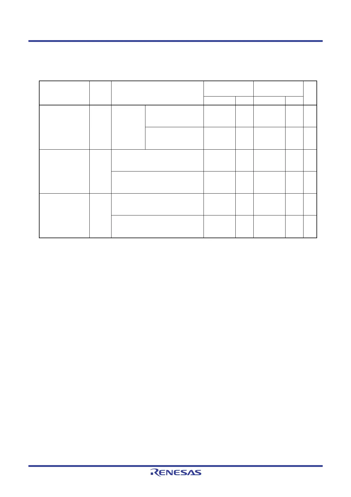
(6) Communication at different potential (1.8 V, 2.5 V, 3 V) (CSI mode) (master mode, SCKp... internal clock
output)
(T
A = ‒40 to +85 °C, 1.8 V ≤ VDD ≤ 3.6 V, VSS = 0 V) (1/3)
Parameter Symbol Conditions HS (high-speed main)
mode
LS (low-speed main)
mode
Unit
MIN. MAX. MIN. MAX.
SCKp cycle time t
KCY1 tKCY1 ≥ 4/fCLK 2.7 V ≤ VDD < 3.6 V,
2.3 V
≤ Vb ≤ 2.7 V,
Cb = 30 pF, Rb = 2.7 kΩ
500 1150 ns
1.8 V
≤ VDD < 3.3 V,
1.6 V
≤ Vb ≤ 2.0 V
Note
,
Cb = 30 pF, Rb = 5.5 kΩ
1150 1150 ns
SCKp high-level width t
KH1 2.7 V ≤ VDD < 3.6 V,
2.3 V
≤ Vb ≤ 2.7 V,
Cb = 30 pF, Rb = 2.7 kΩ
t
KCY1/2 ‒ 170 tKCY1/2 ‒ 170 ns
1.8 V
≤ VDD < 3.3 V,
1.6 V
≤ Vb ≤ 2.0 V
Note
,
Cb = 30 pF, Rb = 5.5 kΩ
t
KCY1/2 ‒ 458 tKCY1/2 ‒ 458 ns
SCKp low-level width t
KL1 2.7 V ≤ VDD < 3.6 V,
2.3 V
≤ Vb ≤ 2.7 V,
Cb = 30 pF, Rb = 2.7 kΩ
t
KCY1/2 ‒ 18 tKCY1/2 ‒ 50 ns
1.8 V
≤ VDD < 3.3 V,
1.6 V
≤ Vb ≤ 2.0 V
Note
,
Cb = 30 pF, Rb = 5.5 kΩ
t
KCY1/2 ‒ 50 tKCY1/2 ‒ 50 ns
 Loading...


