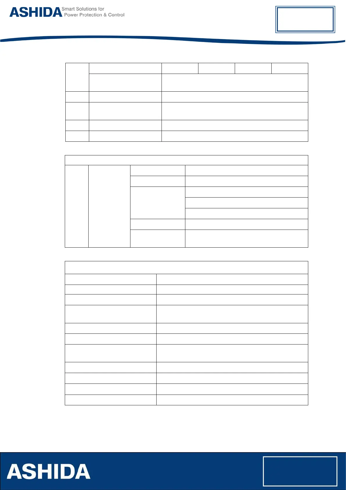
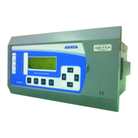
ADR233B
Ref ID : ADR233B/IM/I&S
Rev No. : 05
Page No. : 34 of 479
II.
Threshold Voltage for DC 18 VDC 35 VDC 77 VDC 154 VDC
Maximum operating voltage
range (RMS Voltage)
250 VDC
III.
Drop out Within 85% of threshold voltage value
IV.
VA Burden of Opto Isolated
Status Input
For each status < 1.5 Watt / VA
V.
Filtering Time < 40ms
VI.
Logic input recognition time : For all Status filtering time + 5ms ± 5 ms
Output contact:
I.
Non Latching
contact
Continuous 5A/250Vac
Make & carry 30Amp for 3sec AC /DC
Breaking capacity AC- 1250VA max @ 250V(PF 0.4)
DC- 100W Resistive max. 5A or 300V
50 Watt Inductive (L/R 45ms) max. 5A or 300V
Operating Time <10msec
Minimum no. of
operations
10,000 operation loaded condition & unloaded
100,000 operations
Processing Specifications and Oscillography:
AC Voltages and Currents Inputs : 32 samples per power system cycle
Processor: : 32 bits
ADC resolution : 16 bits
Frequency band : 45 to 55Hz for 50Hz and 55 to 65Hz for 60Hz power system
cycle
Protection and control processing : 1/4 times per power system cycle
Oscillography : 32 samples per cycle / 16 samples per cycle selectable
Length : 1.5sec for RAW or 3 sec for 16 samples of each recording
(Maximum 10 nos. of recording)
Oscillography triggering : Programmable 5% to 95%
Time stamp resolution : 1ms
No. of Analogue Channel : 14 Channels (User assignable through RTV2)
No. of Digital Channel : 32 Channels (User assignable through RTV2)