Maintenance-Object Repair Procedures
555-233-143
8-1384 Issue 1 May 2002
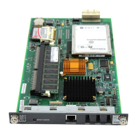
SNC-BD (Switch Node Clock Circuit
Pack)
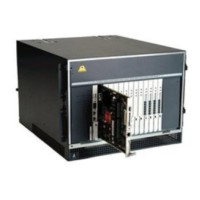
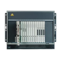
The Switch Node Clock (SNC) TN572 circuit pack is part of the Center Stage
Switch (CSS) configuration. It resides in a switch node carrier that alone or with
other switch nodes make up a CSS. In a high-reliability system (duplicated server
and control network, unduplicated PNC), each SNC is duplicated such that there
are two SNCs in each switch node carrier. In a critical-reliability system
(duplicated server, control network, and PNC), each switch node is fully
duplicated, and there is one SNC in each switch node carrier. SNCs are placed in
slots 10 and 12 of the switch node carrier.
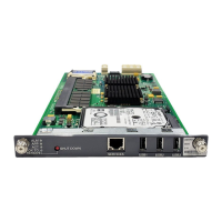
The active SNC communicates with each circuit pack in the switch node carrier
over the serial channel bus on the backplane. In addition, the active SNC
provides timing to the circuit packs in the switch node carrier via the clock buses.
The active SNC uses Timing Priority Number (TPN) links with each Switch Node
Interface (SNI) and the other SNC to receive and distribute TPNs. TPNs are used
for setting up the correct timing distribution for the switch node carrier. The active
SNC receives timing for the switch node carrier from each SNI circuit pack in the
carrier and chooses the SNI with the best timing reference for the switch node
carrier timing signal the SNC puts out on the clock buses. The timing reference
for each SNI is derived from the fiber signal to each SNI. The active SNC
chooses the SNI to receive timing from by choosing the SNI with the lowest
numbered TPN which means that the SNI is closest to the system timing source.
The active SNC also verifies that the SNI reference signal is good before using
that SNI as the timing reference for the switch node carrier. The active SNC then
supplies this timing over the clock buses on the backplane to every SNI and SNC
circuit pack in the carrier. For more information about timing synchronization
(including how the SNC fits into the overall synchronization configuration), see
‘‘SYNC (Port-Network Synchronization)’’ on page 8-1509.
MO’s Name (in
Alarm Log)
Alarm
Level
Initial SAT Command to
Run
1
1. UU is the universal cabinet number (1–64 for ATM PNC, 1–44 for CSS PNC). C is the carrier
designation (A, B, C, D, or E). SS is the number of the slot where the circuit pack resides
(10 or 12).
Full Name of MO
SNC-BD MAJOR test board UUCSS s SNC Circuit Pack
SNC-BD MINOR test board UUCSS s SNC Circuit Pack
 Loading...