© 2004 Microchip Technology Inc. DS70061C-page 14-15
Section 14. Output Compare
Output
Compare
14
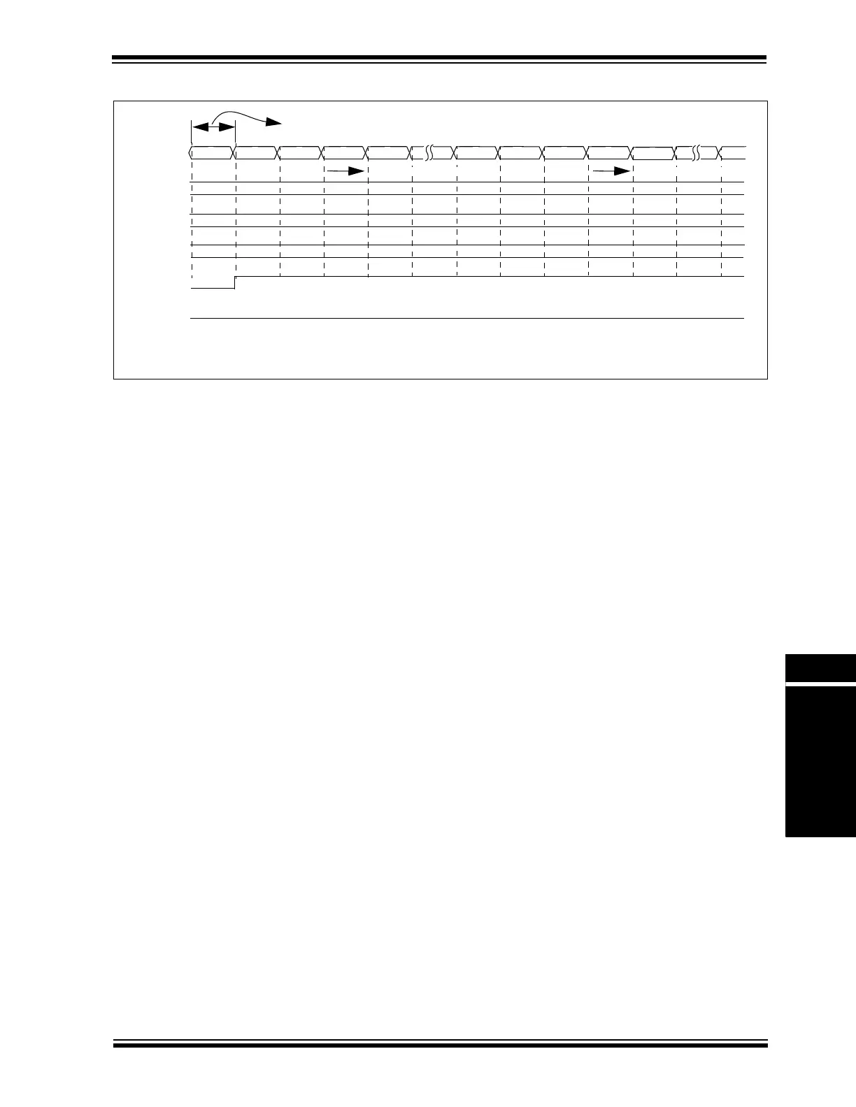
Figure 14-9: Dual Compare Mode: Continuous Output Pulse (PR2 = OCxRS)
14.3.2.5 Setup for Continuous Output Pulse Generation
When control bits OCxM<2:0> (OCxCON<2:0>) are set to ‘101’, the selected output compare
channel initializes the OCx pin to the low state and generates output pulses on each and every
compare match event.
For the user to configure the module for the generation of a continuous stream of output pulses,
the following steps are required (these steps assume timer source is initially turned off, but this
is not a requirement for the module operation):
1. Determine the instruction clock cycle time. Take into account the frequency of the external
clock to the timer source (if one is used) and the timer prescaler settings.
2. Calculate time to the rising edge of the output pulse relative to the TMRy start value
(0x0000).
3. Calculate the time to the falling edge of the pulse, based on the desired pulse width and
the time to the rising edge of the pulse.
4. Write the values computed in step 2 and 3 above into the compare register, OCxR, and
the secondary compare register, OCxRS, respectively.
5. Set timer period register, PRy, to value equal to or greater than value in OCxRS, the
secondary compare register.
6. Set OCM<2:0> = ‘101’ and the OCTSEL (OCxCON<3>) bit to the desired timer source.
The OCx pin state will now be driven low.
7. Enable the compare time base by setting the TON (TyCON<15>) bit to ‘1’.
8. Upon the first match between TMRy and OCxR, the OCx pin will be driven high.
9. When the compare time base, TMRy, matches the secondary compare register, OCxRS,
the second and trailing edge (high-to-low) of the pulse is driven onto the OCx pin.
10. As a result of the second compare match event, the OCxIF interrupt flag bit set.
11. When the compare time base and the value in its respective period register match, the
TMRy register resets to 0x0000 and resumes counting.
12. Steps 8 through 11 are repeated and a continuous stream of pulses is generated,
indefinitely. The OCxIF flag is set on each OCxRS-TMRy compare match event.
OCxIF
3003
3001 3002 3003 00003000
TMRy
3002
1 Instruction Clock Period
3003
3000
PRy
OCxR
3000
OCx pin
3003
OCxRS
3001
3000
0000
TMRy Resets Here TMRy Resets Here
Note 1: An ‘x’ represents the output compare channel number. A ‘y’ represents the time base number.
2: OCxR = Compare Register, OCxRS = Secondary Compare Register.
Compare Interrupt does not Occur