dsPIC30F Family Reference Manual
DS70061C-page 14-14 © 2004 Microchip Technology Inc.
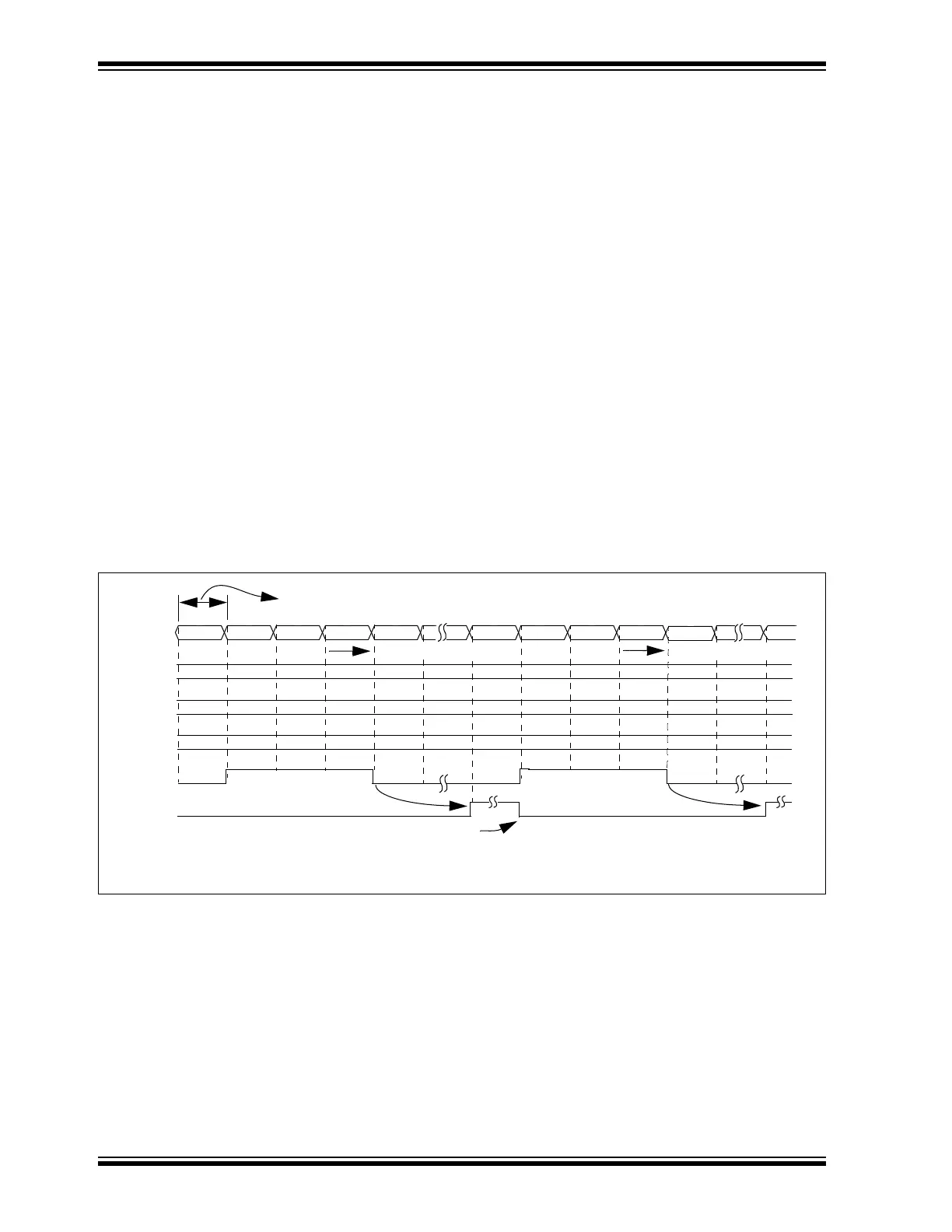
14.3.2.4 Dual Compare Mode: Continuous Output Pulses
To configure the output compare module for this mode, set control bits OCM<2:0> = ‘101’. In
addition, the compare time base must be selected and enabled. Once this mode has been
enabled, the output pin, OCx, will be driven low and remain low until a match occurs between the
compare time base and OCxR register. Referring to Figure 14-8 and Figure 14.3.2.5, there are
some key timing events to note:
• The OCx pin is driven high one instruction clock after the compare match occurs between
the compare time base and OCxR register. The OCx pin will remain high until the next
match event occurs between the time base and the OCxRS register, at which time the pin
will be driven low. This pulse generation sequence of a low-to-high and high-to-low edge
will repeat on the OCx pin without further user intervention.
• Continuous pulses will be generated on the OCx pin until a mode change is made, or the
module is disabled.
• The compare time base will count up to the value contained in the associated period
register and then reset to 0x0000 on the next instruction clock.
• If the compare time base period register value is less than the OCxRS register value, then
no falling edge is generated. The OCx pin will remain high until OCxRS <= PR2, a mode
change is made, or the device is reset.
• The respective channel interrupt flag, OCxIF, is asserted 2 instruction clocks after the OCx
pin is driven low (falling edge of single pulse).
Figure 14-8 depicts the General Dual Compare mode generating a continuous output pulse.
Figure 14.3.2.5 depicts another timing example where OCxRS > PRy. In this example, no falling
edge of the pulse is generated, since the time base will reset before counting up to the contents
of OCxRS.
Figure 14-8: Dual Compare Mode: Continuous Output Pulse (PR2 = OCxRS)
OCxIF
3003
3001 3002 3003 00003000
TMRy
3002
Cleared by User
1 Instruction Clock Period
2 TCY
3003
3000
PRy
OCxR
3000
OCx pin
3003
OCxRS
3001
3000
0000
2 TCY
TMRy Resets Here
TMRy Resets Here
Note 1: An ‘x’ represents the output compare channel number. A ‘y’ represents the time base number.
2: OCxR = Compare Register, OCxRS = Secondary Compare Register.