RL78/G1H CHAPTER 13 A/D CONVERTER
R01UH0575EJ0120 Rev. 1.20 Page 292 of 920
Dec 22, 2016
Note 1. For the second and subsequent conversion in sequential conversion mode, the conversion start time and stabilization
wait time for A/D power supply do not occur after a hardware trigger is detected (see
Table 13 - 3).
Note 2. These are the numbers of clock cycles when conversion is with 10-bit resolution. When eight-bit resolution is selected,
the values are shorter by two cycles of the conversion clock (f
AD).
Caution 1. The A/D conversion time must also be within the relevant range of conversion times (tCONV) described in 31.6.1
A/D converter characteristics.
Note that the conversion time (t
CONV) does not include the A/D power supply stabilization wait time.
Caution 2. Rewrite the FR2 to FR0, LV1 and LV0 bits to other than the same data while conversion is stopped (ADCS = 0,
ADCE = 0).
Caution 3. The above conversion time does not include conversion state time. Conversion state time add in the first
conversion. Select conversion time, taking clock frequency errors into consideration.
Caution 4. When hardware trigger wait mode, specify the conversion time, including the A/D power supply stabilization wait
time from the hardware trigger detection.
Remark
fCLK: CPU/peripheral hardware clock frequency
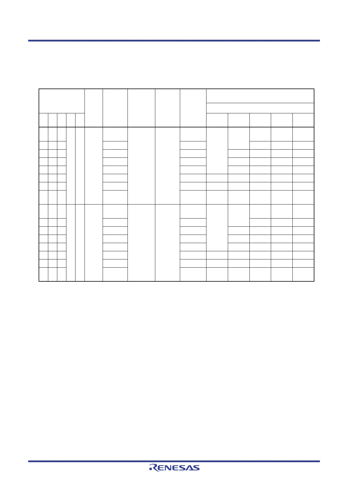
Table 13 - 5 A/D Conversion Time Selection (3/4)
(3) When there is A/D power supply stabilization wait time Normal mode 1, 2
(hardware trigger wait mode
Note 1
)
A/D Converter Mode
Register 0 (ADM0)
Mode Conversion
Clock
(f
AD)
Number of
A/D Power
Supply
Stabilization
Wait Clock
Number of
Conversion
Clock
Note 2
A/D Power
Supply
Stabilization
Wait Time +
Conversion
Time
A/D Power Supply Stabilization Wait Time
+ Conversion Time at 10-Bit Resolution
2.7 V
≤ VDD ≤ 3.6 V
FR2 FR1 FR0 LV1 LV0 f
CLK =
1 MHz
fCLK =
4 MHz
fCLK =
8 MHz
fCLK =
16 MHz
fCLK =
32 MHz
00000Normal 1f
CLK/64 8 fAD 19 fAD
(number of
sampling
clock: 7 f
AD)
1728/f
CLK Setting
prohibited
Setting
prohibited
Setting
prohibited
108 μs 54 μs
001 f
CLK/32 864/fCLK 108 μs54 μs 27 μs
010 f
CLK/16 432/fCLK 108 μs54 μs27 μs 13.5 μs
011 f
CLK/8 216/fCLK 54 μs27 μs 13.5 μs6.75 μs
100 f
CLK/6 162/fCLK 40.5 μs 20.25 μs 10.125 μs 5.0625 μs
101 f
CLK/5 135/fCLK 135 μs33.75 μs 16.875 μs 8.4375 μs 4.21875 μs
110 f
CLK/4 108/fCLK 108 μs27 μs 13.5 μs6.75 μs 3.375 μs
111 f
CLK/2 54/fCLK 54 μs 13.5 μs 6.75 μs 3.375 μsSetting
prohibited
00001Normal 2f
CLK/64 8 fAD 17 fAD
(number of
sampling
clock: 5 f
AD)
1600/f
CLK Setting
prohibited
Setting
prohibited
Setting
prohibited
100 μs 50 μs
001 f
CLK/32 800/fCLK 100 μs50 μs 25 μs
010 f
CLK/16 400/fCLK 100 μs50 μs25 μs 12.5 μs
011 f
CLK/8 200/fCLK 50 μs25 μs 12.5 μs6.25 μs
100 f
CLK/6 150/fCLK 37.5 μs 18.75 μs 9.375 μs 4.6875 μs
101 f
CLK/5 125/fCLK 125 μs31.25 μs 15.625 μs 7.8125 μs 3.90625 μs
110 f
CLK/4 100/fCLK 100 μs25 μs 12.5 μs6.25 μs 3.125 μs
111 f
CLK/2 50/fCLK 50 μs 12.5 μs 6.25 μs 3.125 μsSetting
prohibited
 Loading...


