RL78/G1H CHAPTER 31 ELECTRICAL SPECIFICATIONS
R01UH0575EJ0120 Rev. 1.20 Page 880 of 920
Dec 22, 2016
Note 1. Use it with VDD ≥ Vb.
Note 2. The maximum operating frequencies of the CPU/peripheral hardware clock (fCLK) are:
HS (high-speed main) mode: 32 MHz (2.7 V
≤ VDD ≤ 3.6 V)
16 MHz (2.4 V
≤ VDD ≤ 3.6 V)
LS (low-speed main) mode: 8 MHz (1.8 V
≤ VDD ≤ 3.6 V)
Caution Select the TTL input buffer for the RxDq pin and the N-ch open drain output (VDD tolerance) mode for the TxDq
pin by using port input mode register g (PIMg) and port output mode register g (POMg). For V
IH and VIL, see the
DC characteristics with TTL input buffer selected.
Remark 1.
Vb [V]: Communication line voltage
Remark 2. q: UART number (q = 1, 3), g: PIM and POM number (g = 0, 14)
Remark 3. fMCK: Serial array unit operation clock frequency
(Operation clock to be set by the CKSmn bit of serial mode register mn (SMRmn). m: Unit number,
n: Channel number (mn = 02, 03, 12, 13))
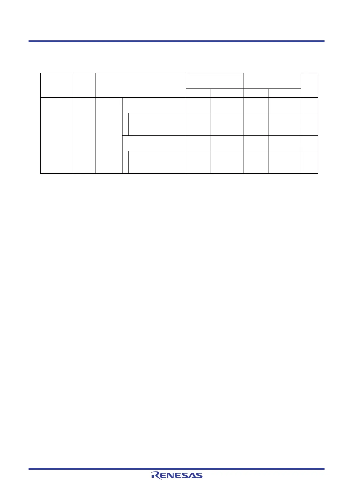
(5) Communication at different potential (1.8 V, 2.5 V, 3 V) (UART mode)
(T
A = ‒40 to +85 °C, 1.8 V ≤ VDD ≤ 3.6 V, VSS = 0 V)
Parameter Symbol Conditions HS (high-speed main)
mode
LS (low-speed main)
mode
Unit
MIN. MAX. MIN. MAX.
Transfer rate reception 2.7 V
≤ VDD < 3.6 V,
2.3 V
≤ Vb ≤ 2.7 V
f
MCK/6 fMCK/6 bps
Theoretical value of the
maximum transfer rate
f
MCK = fCLK
Note 2
5.3 1.3 Mbps
1.8 V
≤ VDD < 3.3 V,
1.8 V
≤ Vb ≤ 2.0 V
f
MCK/6
Note 1
fMCK/6
Note 1
bps
Theoretical value of the
maximum transfer rate
f
MCK = fCLK
Note 2
5.3 1.3 Mbps
 Loading...


