RM0440 Rev 4 1137/2126
RM0440 Advanced-control timers (TIM1/TIM8/TIM20)
1226
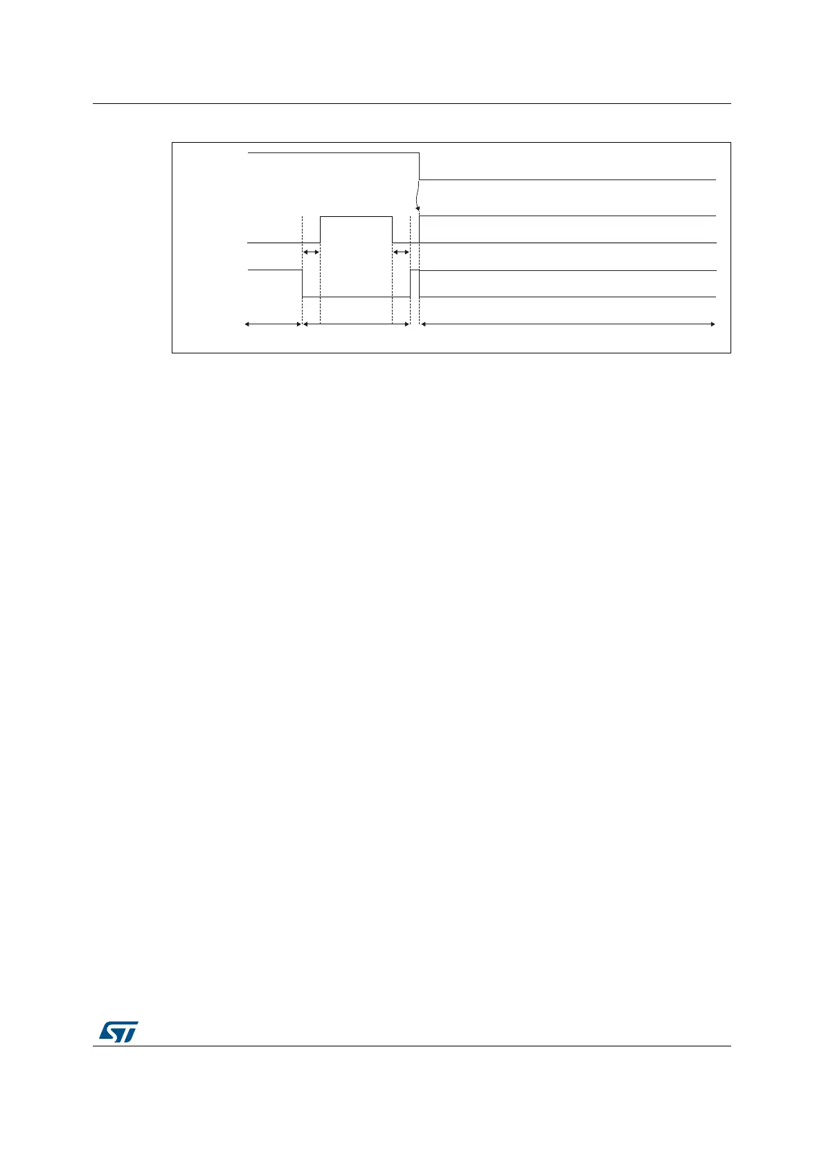
Figure 319. PWM output state following tim_brk assertion (OSSI=0)
28.3.19 Bidirectional break inputs
The TIM1/TIM8/TIM20 are featuring bidirectional break I/Os, as represented on Figure 320.
This provides support for:
• A board-level global break signal available for signaling faults to external MCUs or gate
drivers, with a unique pin being both an input and an output status pin
• Internal break sources and multiple external open drain sources ORed together to
trigger a unique break event, when multiple internal and external break sources must
be merged
The tim_brk and tim_brk2 inputs are configured in bidirectional mode using the BKBID and
BK2BID bits in the TIMxBDTR register. The BKBID programming bits can be locked in read-
only mode using the LOCK bits in the TIMxBDTR register (in LOCK level 1 or above).
The bidirectional mode is available for both the tim_brk and tim_brk2 inputs, and require the
I/O to be configured in open-drain mode with active low polarity (using BKINP, BKP, BK2INP
and BK2P bits). Any break request coming either from system (e.g. CSS), from on-chip
peripherals or from break inputs forces a low level on the break input to signal the fault
event. The bidirectional mode is inhibited if the polarity bits are not correctly set (active high
polarity), for safety purposes.
The break software events (BG and B2G) also cause the break I/O to be forced to '0' to
indicate to the external components that the timer is entered in break state. However, this is
valid only if the break is enabled (BKE or B2KE = 1). When a software break event is
generated with BKE or B2KE = 0), the outputs are put in safe state and the break flag is set,
but there is no effect on the TIMx_BKIN and TIMx_BKIN2 I/Os.
A safe disarming mechanism prevents the system to be definitively locked-up (a low level on
the break input triggers a break which enforces a low level on the same input).
When the BKDSRM (BK2DSRM) bit is set to 1, this releases the break output to clear a fault
signal and to give the possibility to re-arm the system.
At no point the break protection circuitry can be disabled:
• The break input path is always active: a break event will be active even if the BKDSRM
(BK2DSRM) bit is set and the open drain control is released. This will prevent the PWM
output to be re-started as long as the break condition is present.
• The BKDSRM (BK2DSRM) bit cannot disarm the break protection as long as the
outputs are enabled (MOE bit is set) (see Table 259).
MSv62339V1
tim_brk
tim_ocx
I/O state
Deadtime
Active Inactive Disabled
I/O state defined by the GPIO controller (HI-Z)
I/O state defined by the GPIO controller (HI-Z)
tim_ocxn
 Loading...


