RM0440 Rev 4 523/2126
RM0440 Flexible static memory controller (FSMC)
571
The maximum capacity is 512 Mbits (26 address lines).
19.6.2 Supported memories and transactions
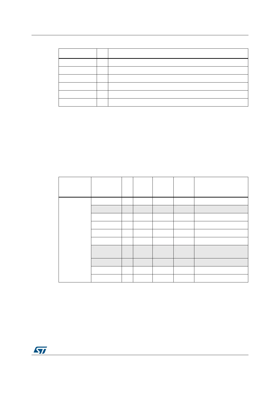
Table 128 below shows an example of the supported devices, access modes and
transactions when the memory data bus is 16-bit wide for NOR Flash memory, PSRAM and
SRAM. The transactions not allowed (or not supported) by the FMC are shown in gray in
this example.
NE[x] O Chip select, x = 1..4 (called NCE by PSRAM (CellularRAM™ i.e. CRAM))
NOE O Output enable
NWE O Write enable
NL(= NADV) O Address valid PSRAM input (memory signal name: NADV)
NWAIT I PSRAM wait input signal to the FMC
NBL[1:0] O Byte lane output. Byte 0 and Byte 1 control (upper and lower byte enable)
Table 127. 16-Bit multiplexed I/O PSRAM (continued)
FMC signal name I/O Function
Table 128. NOR Flash/PSRAM: example of supported memories
and transactions
Device Mode R/W
AHB
data
size
Memory
data size
Allowed/
not
allowed
Comments
NOR Flash
(muxed I/Os
and nonmuxed
I/Os)
Asynchronous R 8 16 Y -
Asynchronous W 8 16 N -
Asynchronous R 16 16 Y -
Asynchronous W 16 16 Y -
Asynchronous R 32 16 Y Split into 2 FMC accesses
Asynchronous W 32 16 Y Split into 2 FMC accesses
Asynchronous
page
R - 16 N Mode is not supported
Synchronous R 8 16 N -
Synchronous R 16 16 Y -
Synchronous R 32 16 Y -