Embedded Flash memory (FLASH) for category 2 devices RM0440
214/2126 RM0440 Rev 4
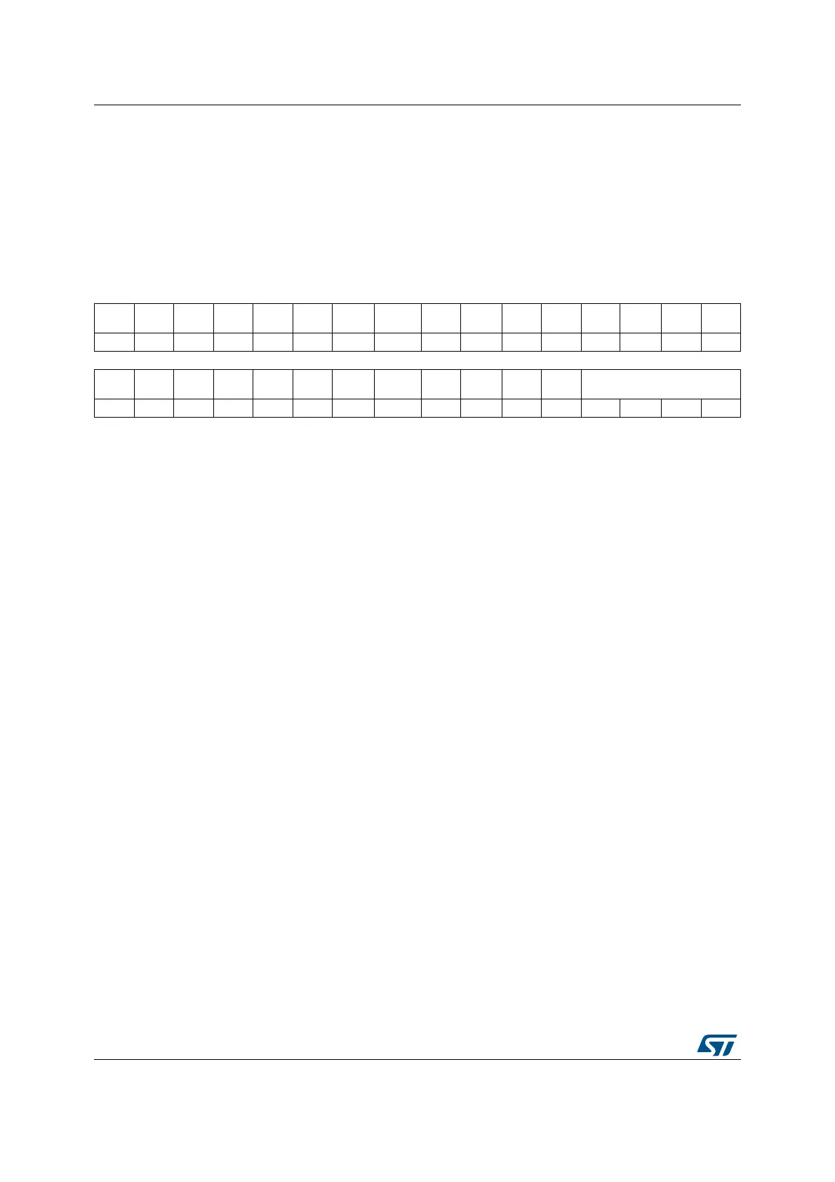
5.7 FLASH registers
5.7.1 Flash access control register (FLASH_ACR)
Address offset: 0x00
Reset value: 0x0000 0600
Access: no wait state, word, half-word and byte access
--
31 30 29 28 27 26 25 24 23 22 21 20 19 18 17 16
Res. Res. Res. Res. Res. Res. Res. Res. Res. Res. Res. Res. Res.
DBG_
SWEN
Res. Res.
rw
15 14 13 12 11 10 9 8 7 6 5 4 3 2 1 0
Res.
SLEEP
_PD
RUN_
PD
DCRST ICRST DCEN ICEN PRFTEN Res. Res. Res. Res. LATENCY[3:0]
rw rw rw rw rw rw rw rw rw rw rw
Bits 31:19 Reserved, must be kept at reset value.
Bit 18 DBG_SWEN: Debug software enable
SW may use this bit to enable/disable the debugger.
0: Debugger disabled
1: Debugger enabled
Bits 17:15 Reserved, must be kept at reset value.
Bit 14 SLEEP_PD: Flash Power-down mode during Sleep or Low-power sleep mode
This bit determines whether the flash memory is in Power-down mode or Idle
mode when the device is in Sleep or Low-power sleep mode.
0: Flash in Idle mode during Sleep and Low-power sleep modes
1: Flash in Power-down mode during Sleep and Low-power sleep modes
Caution: The flash must not be put in power-down while a program or an erase
operation is on-going.
Bit 13 RUN_PD: Flash Power-down mode during Run or Low-power run mode
This bit is write-protected with FLASH_PDKEYR.
This bit determines whether the flash memory is in Power-down mode or Idle
mode when the device is in Run or Low-power run mode. The flash memory can
be put in power-down mode only when the code is executed from RAM. The
Flash must not be accessed when RUN_PD is set.
0: Flash in Idle mode
1: Flash in Power-down mode
Caution: The flash must not be put in power-down while a program or an erase
operation is on-going.
Bit 12 DCRST: Data cache reset
0: Data cache is not reset
1: Data cache is reset
This bit can be written only when the data cache is disabled.