RM0440 Rev 4 1201/2126
RM0440 Advanced-control timers (TIM1/TIM8/TIM20)
1226
Note: The state of the external I/O pins connected to the complementary tim_ocx and tim_ocxn
channels depends on the tim_ocx and tim_ocxn channel state and the GPIO registers.
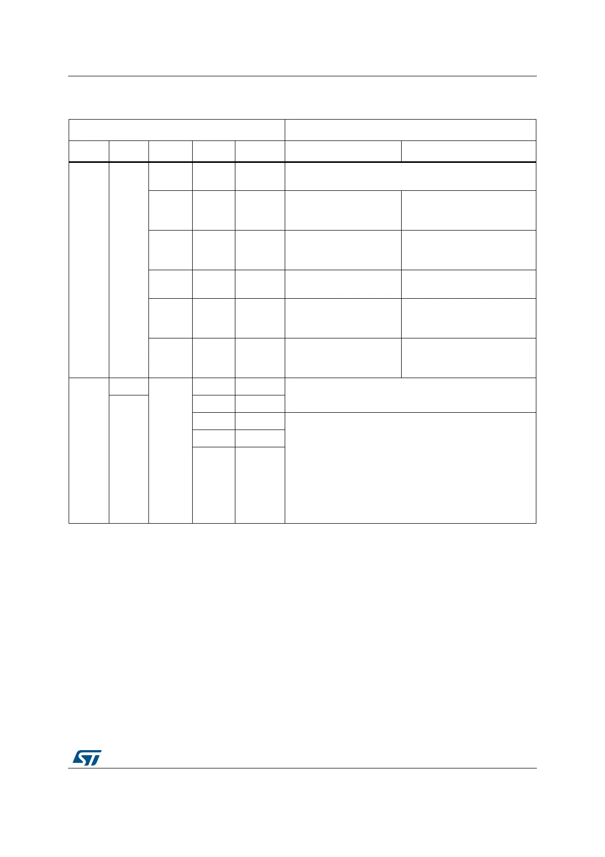
Table 265. Output control bits for complementary tim_ocx and tim_ocxn channels
with break feature
Control bits Output states
(1)
MOE bit OSSI bit OSSR bit CCxE bit CCxNE bit tim_ocx output state tim_ocxn output state
1X
X0 0
Output disabled (not driven by the timer: Hi-Z)
tim_ocx=0, tim_ocxn=0
00 1
Output disabled (not driven
by the timer: Hi-Z)
tim_ocx=0
tim_ocxref + Polarity
tim_ocxn = tim_ocxref xor
CCxNP
01 0
tim_ocxref + Polarity
tim_ocx=tim_ocxref xor
CCxP
Output Disabled (not driven by
the timer: Hi-Z)
tim_ocxn=0
X1 1
OCREF + Polarity + dead-
time
Complementary to OCREF (not
OCREF) + Polarity + dead-time
10 1
Off-State (output enabled
with inactive state)
tim_ocx=CCxP
tim_ocxref + Polarity
tim_ocxn = tim_ocxref x or
CCxNP
11 0
tim_ocxref + Polarity
tim_ocx=tim_ocxref xor
CCxP
Off-State (output enabled with
inactive state)
tim_ocxn=CCxNP
0
0
X
XX
Output disabled (not driven by the timer: Hi-Z).
1
00
0 1 Off-State (output enabled with inactive state)
Asynchronously: tim_ocx=CCxP, tim_ocxn=CCxNP (if
tim_brk or tim_brk2 is triggered).
Then (this is valid only if tim_brk is triggered), if the clock is
present: tim_ocx=OISx and tim_ocxn=OISxN after a dead-
time, assuming that OISx and OISxN do not correspond to
OCX and tim_ocxn both in active state (may cause a short
circuit when driving switches in half-bridge configuration).
Note: tim_brk2 can only be used if OSSI = OSSR = 1.
10
11
1. When both outputs of a channel are not used (control taken over by GPIO), the OISx, OISxN, CCxP and CCxNP bits must
be kept cleared.