RM0440 Rev 4 1369/2126
RM0440 General-purpose timers (TIM15/TIM16/TIM17)
1445
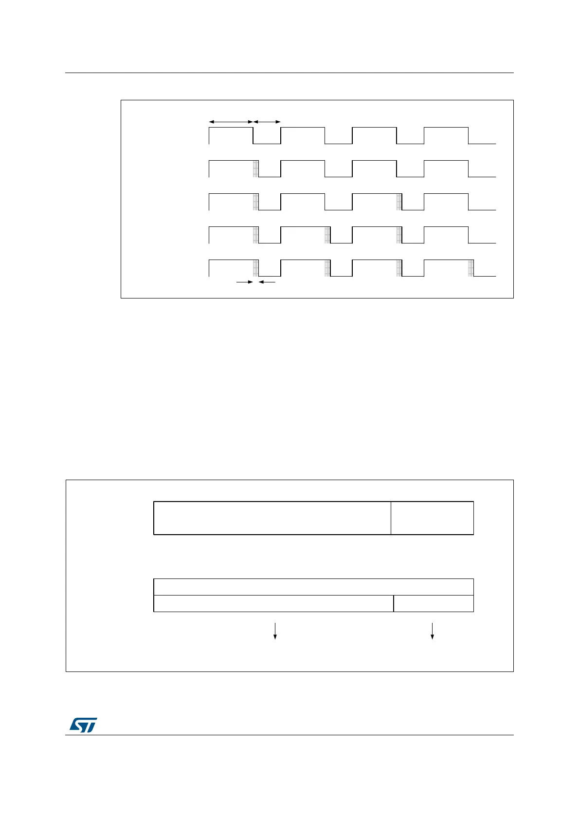
Figure 460. Dithering principle
When the dithering mode is enabled, the register coding is changed as following (see
Figure 461 for example):
• the 4 LSBs are coding for the enhanced resolution part (fractional part)
• the MSBs are left-shifted to the bits 19:4 and are coding for the base value.
Note: The ARR and CCR values will be updated automatically if the DITHEN bit is set / reset (for
instance, if ARR= 0x05 with DITHEN=0, it will be updated to ARR = 0x50 with DITHEN = 1).
The following sequence must be followed when resetting the DITHEN bit:
1. CEN and ARPE bits must be reset
2. The ARR[3:0] bits must be reset
3. The DITHEN bit must be reset
4. The CCIF flags must be cleared
5. The CEN bit can be set (eventually with ARPE = 1).
Figure 461. Data format and register coding in dithering mode
The minimum frequency is given by the following formula:
MSv45752V1
1 clock cycle
Average duty cycle
75
DC = 7/5
DC = (7+¼)/5
DC = (7+½)/5
DC = (7+¾)/5
DC = 8/5
MSv45753V2
MSB: 16-bits, integer part
LSB: 4-bits
fractional part
326
20 6
Base compare value is 20 during 16 periods
Additional 6 cycles are spread over the
16 periods
Register format in
dithering mode
Example
b0b19
b0b19