Embedded Flash memory (FLASH) for category 2 devices RM0440
212/2126 RM0440 Rev 4
The size of the Securable memory area is defined by the SEC_SIZE1[7:0] bitfield of the
FLASH_SEC register. It can be modified only in RDP Level 0. Its content is erased upon
changing from RDP Level 1 to Level 0, even if it overlaps with PCROP pages.
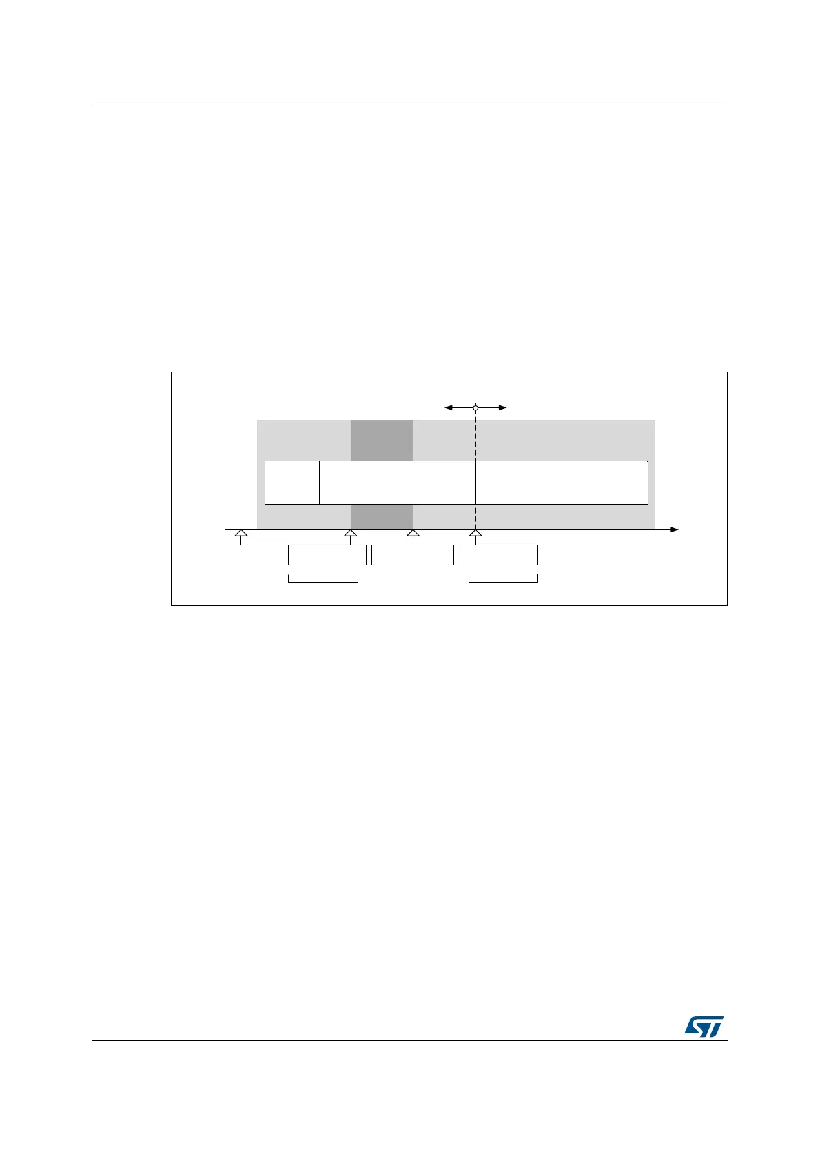
5.5.5 Disabling core debug access
For executing sensitive code or manipulating sensitive data in Securable memory area, the
debug access to the core can temporarily be disabled.
In RDP level 2, the debugger is disabled by hardware, , but in other RDP levels, the
debugger can be disabled by software using the bit DBG_SWEN in the FLASH_ACR
register.
Figure 11 gives an example of managing DBG_SWEN and SEC_PROT bits.
Figure 11. Example of disabling core debug access
5.5.6 Forcing boot from Flash memory
To increase the security and establish a chain of trust, the BOOT_LOCK option bit of the
FLASH_SEC1R/FLASH_SEC2R register allows forcing the system to boot from the Main
Flash memory regardless the other boot options. It is always possible to set the
BOOT_LOCK bit. However, it is possible to reset it only when:
• RDP is set to Level 0, or
• RDP is set to Level 1, while Level 0 is requested and a full mass-erase is performed.
MSv42192V1
timeline
Debug
enabled
Debug
enabled
Debug
disabled
DBG_SWEN = 0 DBG_SWEN = 1 SEC_PROT = 1
Option
byte
loading
Execution of code
within securable memory
Execution of code
outside securable memory
Power up
SEC_PROT = 1
Securable memory secured
SEC_PROT = 0
Securable memory not secured
Software management