RM0440 Rev 4 2101/2126
RM0440 Debug support (DBG)
2112
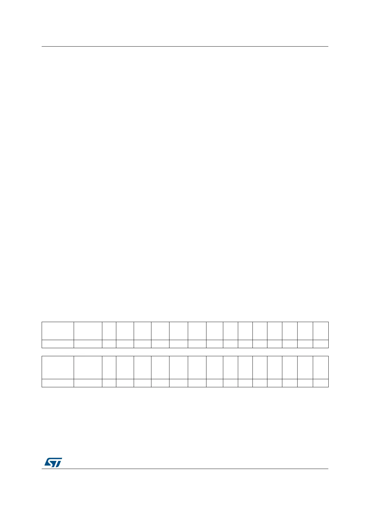
47.16.4 Debug MCU APB1 freeze register1(DBGMCU_APB1FZR1)
Address: 0xE004 2008
Power on reset (POR): 0x0000 0000
System reset: not affected
Access: Only 32-bit access are supported.
Bit 2 DBG_STANDBY: Debug Standby mode
0: (FCLK=Off, HCLK=Off) The whole digital part is unpowered.
From software point of view, exiting from Standby is identical than fetching reset vector
(except a few status bit indicated that the MCU is resuming from Standby)
1: (FCLK=On, HCLK=On) In this case, the digital part is not unpowered and FCLK and
HCLK are provided by the internal RC oscillator which remains active. In addition, the MCU
generate a system reset during Standby mode so that exiting from Standby is identical than
fetching from reset.
Bit 1 DBG_STOP: Debug Stop mode
0: (FCLK=Off, HCLK=Off) In STOP mode, the clock controller disables all clocks (including
HCLK and FCLK). When exiting from STOP mode, the clock configuration is identical to the
one after RESET (CPU clocked by the 8 MHz internal RC oscillator (HSI16)). Consequently,
the software must reprogram the clock controller to enable the PLL, the Xtal, etc.
1: (FCLK=On, HCLK=On) In this case, when entering STOP mode, FCLK and HCLK are
provided by the internal RC oscillator which remains active in STOP mode. When exiting
STOP mode, the software must reprogram the clock controller to enable the PLL, the Xtal,
etc. (in the same way it would do in case of DBG_STOP=0)
Bit 0 DBG_SLEEP: Debug Sleep mode
0: (FCLK=On, HCLK=Off) In Sleep mode, FCLK is clocked by the system clock as
previously configured by the software while HCLK is disabled.
In Sleep mode, the clock controller configuration is not reset and remains in the previously
programmed state. Consequently, when exiting from Sleep mode, the software does not
need to reconfigure the clock controller.
1: (FCLK=On, HCLK=On) In this case, when entering Sleep mode, HCLK is fed by the same
clock that is provided to FCLK (system clock as previously configured by the software).
31 30 29 28 27 26 25 24 23 22 21 20 19 18 17 16
DBG_LPTIM1_
STOP
DBG_I2C3_
STOP
Res. Res. Res. Res. Res. Res. Res.
DBG_
I2C2_
STOP
DBG_
I2C1_
STOP
Res. Res. Res. Res. Res.
rw rw rw rw
15 14 13 12 11 10 9 8 7 6 5 4 3 2 1 0
Res. Res. Res.
DBG_
IWDG_
STOP
DBG_
WWDG
_STOP
DBG_
RTC_
STOP
Res. Res. Res. Res.
DBG_
TIM7
_STO
P
DBG_
TIM6
_STO
P
DBG_
TIM5
_STO
P
DBG_
TIM4_
STOP
DBG_
TIM3_
STOP
DBG_
TIM2_
STOP
rw rw rw rw rw rw rw rw rw
 Loading...


