RM0440 Rev 4 435/2126
RM0440 DMA request multiplexer (DMAMUX)
440
13.6 DMAMUX registers
Refer to the table containing register boundary addresses for the DMAMUX base address.
DMAMUX registers may be accessed per (8-bit) byte, (16-bit) half-word, or (32-bit) word.
The address must be aligned with the data size.
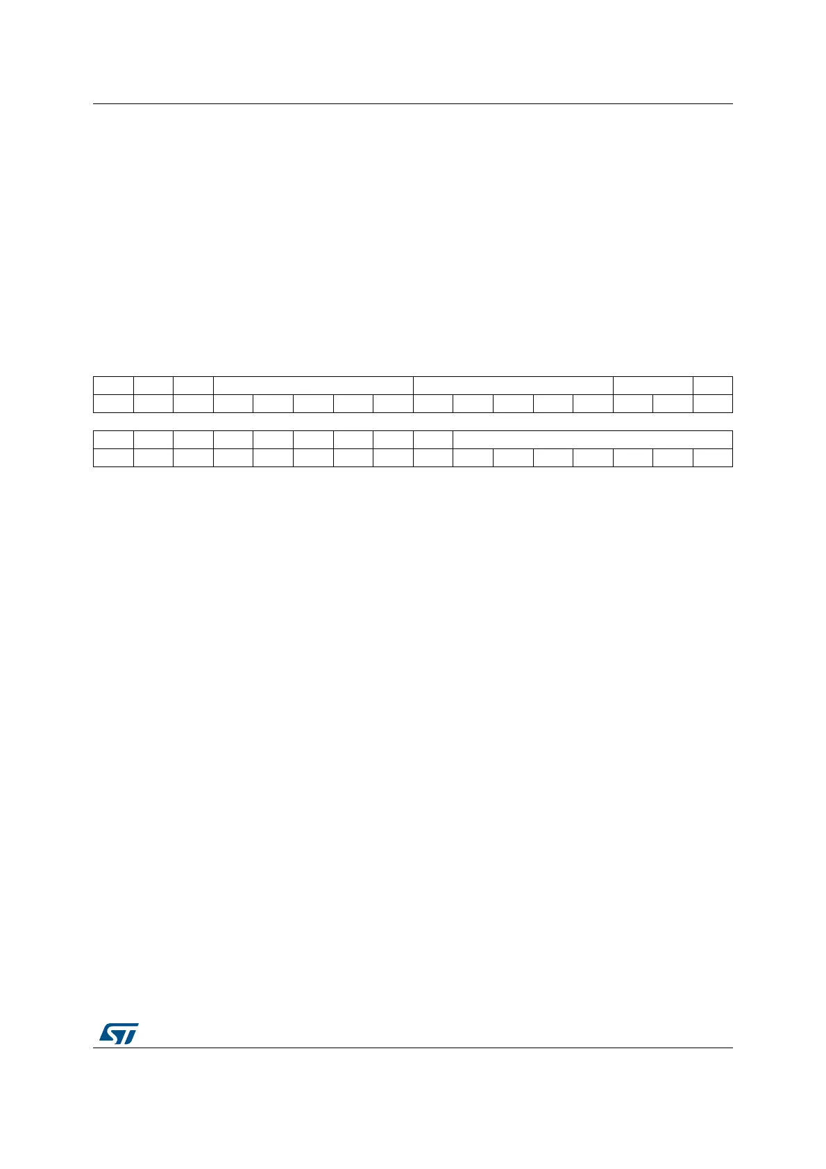
13.6.1 DMAMUX request line multiplexer channel x configuration register
(DMAMUX_CxCR)
Address offset: 0x000 + 0x04 * x (x = 0 to 15)
Reset value: 0x0000 0000
31 30 29 28 27 26 25 24 23 22 21 20 19 18 17 16
Res. Res. Res. SYNC_ID[4:0] NBREQ[4:0] SPOL[1:0] SE
rw rw rw rw rw rw rw rw rw rw rw rw rw
1514131211109876543210
Res. Res. Res. Res. Res. Res. EGE SOIE Res. DMAREQ_ID[6:0]
rw rw rw rw rw rw rw rw rw
Bits 31:29 Reserved, must be kept at reset value.
Bits 28:24 SYNC_ID[4:0]: Synchronization identification
Selects the synchronization input (see ).
Bits 23:19 NBREQ[4:0]: Number of DMA requests minus 1 to forward
Defines the number of DMA requests to forward to the DMA controller after a synchronization
event, and/or the number of DMA requests before an output event is generated.
This field shall only be written when both SE and EGE bits are low.
Bits 18:17 SPOL[1:0]: Synchronization polarity
Defines the edge polarity of the selected synchronization input:
00: no event, i.e. no synchronization nor detection.
01: rising edge
10: falling edge
11: rising and falling edge
Bit 16 SE: Synchronization enable
0: synchronization disabled
1: synchronization enabled
Bits 15:10 Reserved, must be kept at reset value.
Bit 9 EGE: Event generation enable
0: event generation disabled
1: event generation enabled
Bit 8 SOIE: Synchronization overrun interrupt enable
0: interrupt disabled
1: interrupt enabled