Quad-SPI interface (QUADSPI) RM0440
572/2126 RM0440 Rev 4
20 Quad-SPI interface (QUADSPI)
20.1 Introduction
The QUADSPI is a specialized communication interface targeting single, dual or quad SPI
Flash memories. It can operate in any of the three following modes:
• indirect mode: all the operations are performed using the QUADSPI registers
• status polling mode: the external Flash memory status register is periodically read and
an interrupt can be generated in case of flag setting
• memory-mapped mode: the external Flash memory is mapped to the device address
space and is seen by the system as if it was an internal memory
Both throughput and capacity can be increased two-fold using dual-flash mode, where two
Quad-SPI Flash memories are accessed simultaneously.
20.2 QUADSPI main features
• Three functional modes: indirect, status-polling, and memory-mapped
• Dual-flash mode, where 8 bits can be sent/received simultaneously by accessing two
Flash memories in parallel.
• SDR and DDR support
• Fully programmable opcode for both indirect and memory mapped mode
• Fully programmable frame format for both indirect and memory mapped mode
• Integrated FIFO for reception and transmission
• 8, 16, and 32-bit data accesses are allowed
• DMA channel for indirect mode operations
• Interrupt generation on FIFO threshold, timeout, operation complete, and access error
20.3 QUADSPI functional description
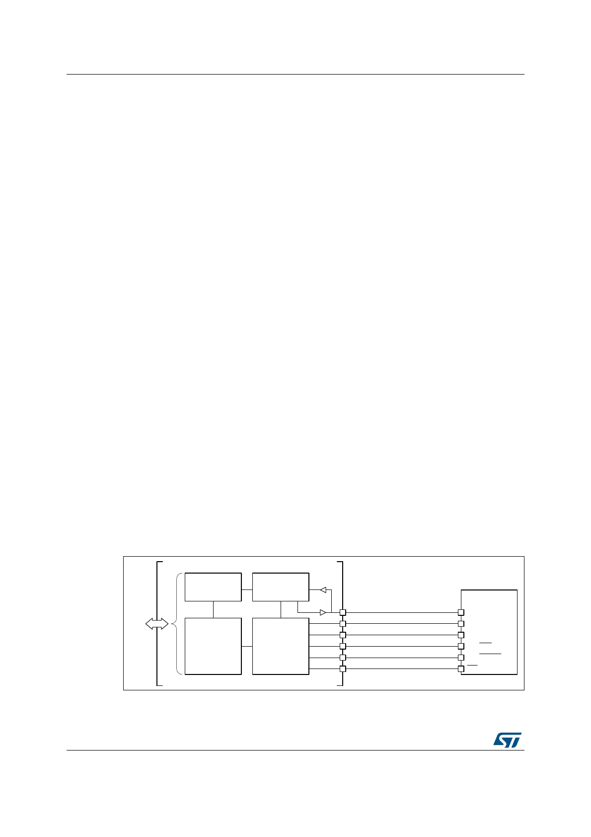
20.3.1 QUADSPI block diagram
Figure 74. QUADSPI block diagram when dual-flash mode is disabled
SPI FLASH
MS35315V1
CLK
BK1_IO0/SO
BK1_IO1/SI
BK1_IO2
BK1_IO3
CLK
Q0/SI
Q1/SO
Q2/WP
Q3/HOLD
BK1_nCS
CS
AHB
Registers /
control
Clock
management
FIFO Shift register
QUADSPI
 Loading...


