B.4 Control Mode Dependent Parameter Default Values
YASKAWA ELECTRIC SIEP C710616 27G YASKAWA AC Drive A1000 Technical Manual 519
B.4 Control Mode Dependent Parameter Default Values
The tables below list parameters that depend on the control mode selection (A1-02 for motor 1, E3-01 for motor 2).
These parameters are initialized to the shown values if the control mode is changed.
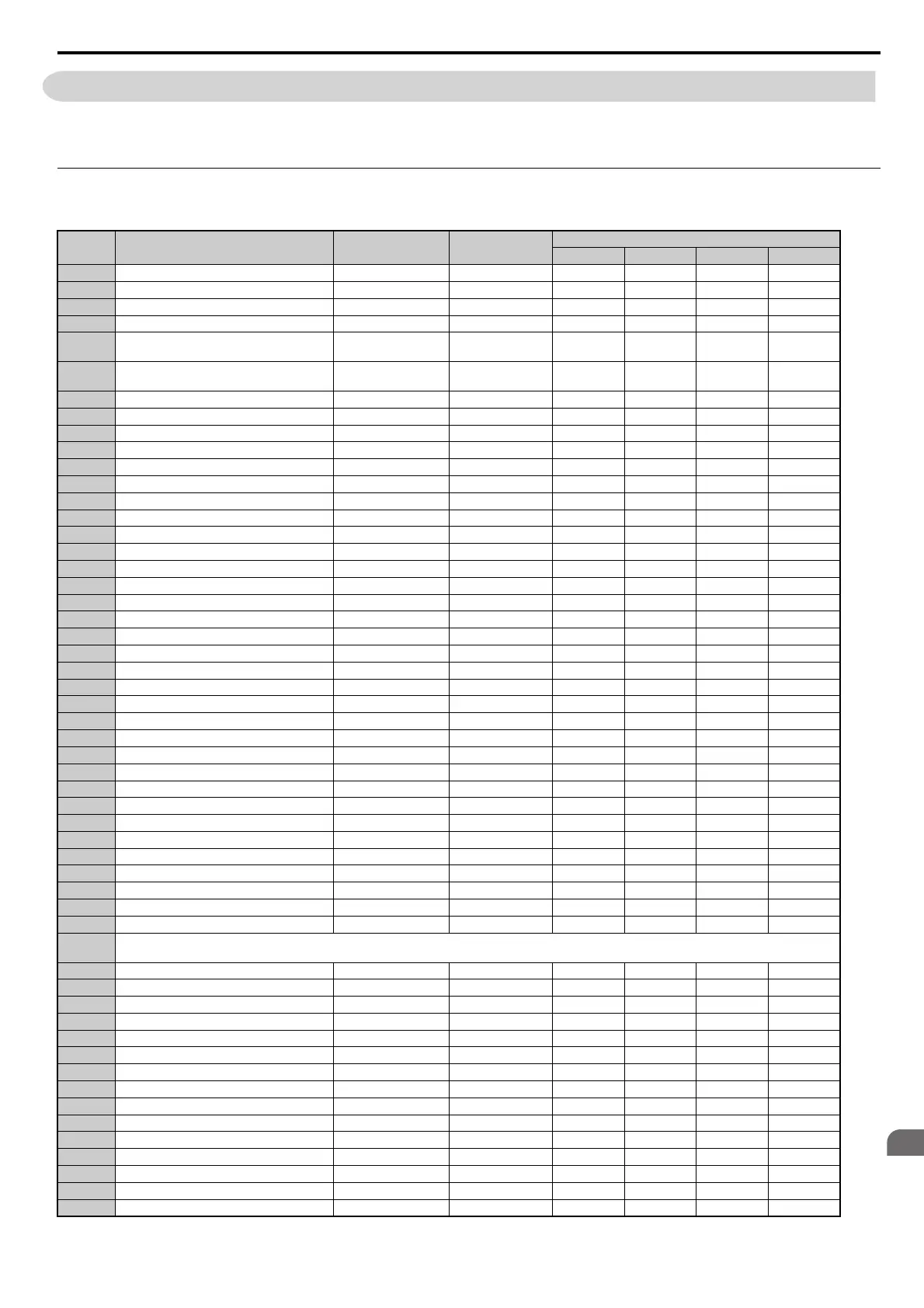
A1-02 (Motor 1 Control Mode) Dependent Parameters
Table B.2 A1-02 (Motor 1 Control Mode) Dependent Parameters and Default Values
No. Name Setting Range Resolution
Control Modes (A1-02)
V/f (0) V/f w/PG (1) OLV (2) CLV (3)
b2-01 DC Injection Braking Start Frequency 0.0 to 10.0 0.1 0.5 Hz 0.5 Hz 0.5 Hz 0.5 Hz
b2-04 DC Injection Braking Time at Stop 0.00 to 10.00 0.01 s 0.50 0.50 0.50 0.50
b3-01 Speed Search Selection at Start 0 to 1 – 0 1 0 –
b3-02 Speed Search Deactivation Current 0 to 200 1% 120 – 100 –
b3-08
Current Control Gain during Speed Search
(Speed Est
imation Type)
0.00 to 6.00 –
<6> <6> <6> <6>
b3-09
Current Control Integral Time during Speed
Sear
ch (Speed Estimation Type)
0.0 to 1000.0 0.1 ms 2.0 ms 2.0 ms 2.0 ms
2.0 ms
b3-14 Bi-Directional Speed Search Selection 0 to 1 – 1 0 1 –
b5-15 PID Sleep Function Start Level 0.0 to 400.0 0.1 0.0 Hz 0.0 Hz 0.0 Hz 0.0 Hz
b6-01 Dwell Reference at Start 0.0 to 400.0 0.1 0.0 Hz 0.0 Hz 0.0 Hz 0.0 Hz
b6-03 Dwell Reference at Stop 0.0 to 400.0 0.1 0.0 Hz 0.0 Hz 0.0 Hz 0.0 Hz
b8-01 Energy Saving Control Selection 0 to 1 – 0 0 0 0
b8-02 Energy Saving Gain 0.0 to 10.0 0.1 – – 0.7 1.0
b8-03 Energy Saving Control Filter Time Constant 0.00 to 10.00 0.01 s – – 0.50 <51> 0.01 <51>
C1-11 Accel/Decel Time Switching Frequency 0.0 to 400.0 0.1 0.0 Hz 0.0 Hz 0.0 Hz 0.0 Hz
C2-01 S-Curve Time at Acceleration Start 0.00 to 10.00 0.01 s 0.20 0.20 0.20 0.20
C3-01 Slip Compensation Gain 0.0 to 2.5 0.1 0.0 – 1.0 1.0
C3-02 Slip Compensation Primary Delay Time 0 to 10000 1 ms 2000 – 200 –
C4-01 Torque Compensation Gain 0.00 to 2.50 0.01 1.00 1.00 1.00 –
C4-02 Torque Compensation Primary Delay Time 0 to 10000 1 ms 200 <54> 200 <54> 20 –
C5-01 ASR Proportional Gain 1 0.00 to 300.00 0.01 – 0.20 – 20.00
C5-02 ASR Integral Time 1 0.000 to 10.000 0.001 s – 0.200 – 0.500
C5-03 ASR Proportional Gain 2 0.00 to 300.00 0.01 – 0.02 – 20.00
C5-04 ASR Integral Time 2 0.000 to 10.000 0.001 s – 0.050 – 0.500
C5-06 ASR Primary Delay Time Constant 0.000 to 0.500 0.001 s – – – 0.004
C5-07 ASR Gain Switching Frequency 0.0 to 400.0 0.1 – – – 0.0 Hz
C6-02 Carrier Frequency Selection 1 to F – 7 <53> 7 <53> 7 <53> 7
d3-01 Jump Frequency 1 0.0 to 400.0 0.1 0.0 Hz 0.0 Hz 0.0 Hz 0.0 Hz
d3-02 Jump Frequency 2 0.0 to 400.0 0.1 0.0 Hz 0.0 Hz 0.0 Hz 0.0 Hz
d3-03 Jump Frequency 3 0.0 to 400.0 0.1 0.0 Hz 0.0 Hz 0.0 Hz 0.0 Hz
d3-04 Jump Frequency Width 0.0 to 20.0 0.1 1.0 Hz 1.0 Hz 1.0 Hz 1.0 Hz
d5-02 Torque Reference Delay Time 0 to 1000 1 ms – – – 0
E1-04 Maximum Output Frequency 40.0 to 400.0 0.1 Hz 60.0 <52> 60.0 60.0 60.0
E1-05 Maximum Voltage <18> 0.0 to 255.0 0.1 V 200 <52> 200 <52> 200 200
E1-06 Base Frequency 0.0 to 400.0 0.1 Hz 60.0 <52> 60.0 <52> 60.0 60.0
E1-07 Middle Output Frequency 0.0 to 400.0 0.1 Hz 3.0 <52> 3.0 <52> 3.0 –
E1-08 Middle Output Frequency Voltage <18> 0.0 to 255.0 0.1 V 15.0 <52> 15.0 <52> 11.0 –
E1-09 Minimum Output Frequency 0.0 to 400.0 0.1 Hz 1.5 <52> 1.5 <52> 0.5 0.0
E1-10 Minimum Output Frequency Voltage <18> 0.0 to 255.0 0.1 V 9.0 9.0 2.0 –
E1-04 to
E1-10
The default setting of these parameters depends on the control mode but also on the drive capacity. Refer to V/f Pattern Default Values on page 522.
F1-01 PG 1 Pulses Per Revolution 0 to 60000 1 ppr – 600 – 600
F1-05 PG 1 Rotation Selection 0 to 1 – – 0 – 0
F1-09 Overspeed Detection Delay Time 0.0 to 2.0 0.1 s – 1.0 – 0.0
L1-01 Motor Overload Protection Selection 0 to 4 – 1 1 1 1
L3-20 DC Bus Voltage Adjustment Gain 0.00 to 5.00 0.01 1.00 1.00 0.30 0.30
L3-21 Accel/Decel Rate Calculation Gain 0.10 to 10.00 0.01 1.00 1.00 1.00 1.00
L3-34 Torque Limit Delay Time 0.000 to 1.000 0.001 s – – – –
L4-01 Speed Agreement Detection Level 0.0 to 400.0 0.1 0.0 Hz 0.0 Hz 0.0 Hz 0.0 Hz
L4-02 Speed Agreement Detection Width 0.0 to 20.0 0.1 2.0 Hz 2.0 Hz 2.0 Hz 2.0 Hz
L4-03 Speed Agreement Detection Level (+/-) -400.0 to 400.0 0.1 0.0 Hz 0.0 Hz 0.0 Hz 0.0 Hz
L4-04 Speed Agreement Detection Width (+/–) 0.0 to 20.0 0.1 2.0 Hz 2.0 Hz 2.0 Hz 2.0 Hz
L8-38 Carrier Frequency Reduction Selection 0 to 2 – <53> <53> <53> <53>
L8-40 Carrier Frequency Reduction Off Delay Time 0.00 to 2.00 0.01 s 0.50 0.50 0.50 0.50
o1-03 Digital Operator Display Selection 0 to 3 – 0 0 0 0
o1-04 V/f Pattern Display Unit 0 to 1 – – – – 0