2-1
IM 701450-01E
2
Explanation of Functions
Chapter 2 Explanation of Functions
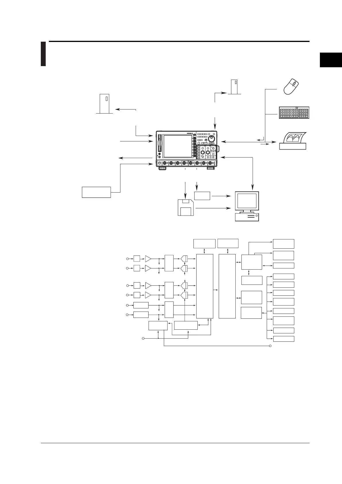
2.1 System Configuration and Block Diagram
System Configuration
Device under
measurement
PC
USB printer
Floppy disk or
Zip disk
USB keyboard
Built-in printer (optional)
External clock input
External trigger input
Trigger gate input
Video signal output (VGA)
Trigger output
Screen image data
Input
USB Peripheral
interface
GP-IB interface
USB interface
Ethernet interface (optional)
Screen image print
USB mouse
Input
COMP
X-Y
PHASE
SEARCH
MENU MENU
SETUP
ESC
FILE
MISC
RESET
SELECT
MATH
SHIFT
GO/NOGO
CURSOR
MEASURE
HISTORY
PRESET
ZOOM
MODE
POSITION
ENHANCED
SIMPLE
LOGIC
CH
1
CH
2
CH
3
CH
4
CH
5
CH
6
CH
7
CH
8
PRINT
ACQ
V/DIV TIME/DIV
START/STOP
IMAGE SAVE
DISPLAY
VERTICAL
TRIGGER
TRIG D
ACTION
DELAY
CLEAR TRACESNAPSHOT
HELP
HORIZONTAL
External
SCSI device
SCSI (optional)
PC card
Analog signal input,
logic signal input (optional)
Waveform data
Setup data
Screen image data
Waveform data
Setup data
Screen image data
Waveform data
Setup data
Screen image data
USB Peripheral
interface
USB storage
Waveform data
Setup data
Screen image data
Block Diagram
CH1
External clock input/
external trigger input/
trigger gate input
ATT
Pre-
AMP
Multiplexer
A/D
Primary
data
processing
circuit
Acquisition
memory
Data
processing
memory
Color LCD
Display
Secondary
data
processing
circuit
Trigger
circuit
Time base
Trigger output
Keyboard
GP-IB
SCSI
FDD or
Zip drive
(Optional)
(Optional)
CH2
CH7
CH8
Primary
memory
Display
memory
Display
processing
circuit
Built-in printer
PC card
(Optional)
Ethernet
VGA video
output
CPU
LOGIC A
LOGIC B
USB
Peripheral
USB
Buffer
Buffer
...
...
...
...
...
Signal Flow
The signal applied to each signal input terminal is first passed to the vertical control circuit
consisting of an attenuator (ATT) and pre-amplifier. At the attenuator and pre-amplifier, the
voltage and amplitude of each input signal is adjusted according to the settings such as the
input coupling, probe attenuation/current-to-voltage conversion ratio, V/div, and offset voltage.
The adjusted input signal is then passed to the multiplexer. The signal input to the
multiplexer is passed to the A/D converter according to the time axis and other settings.
At the A/D converter, the received voltage level is converted into digital values. The digital
data is written to the primary memory by the primary data processing circuit at the sample
rate that matches the time axis setting. The data written to the primary memory is processed
(averaged, for example) by the secondary data processing circuit and written to the
acquisition memory. The data written to the acquisition memory is converted into waveform display
data by the secondary data processing circuit, transferred to the waveform processing circuit, and
stored in the display memory. The waveforms are displayed on the LCD using the data stored in the
display memory.
 Loading...