RM0440 Rev 4 1975/2126
RM0440 FD controller area network (FDCAN)
2008
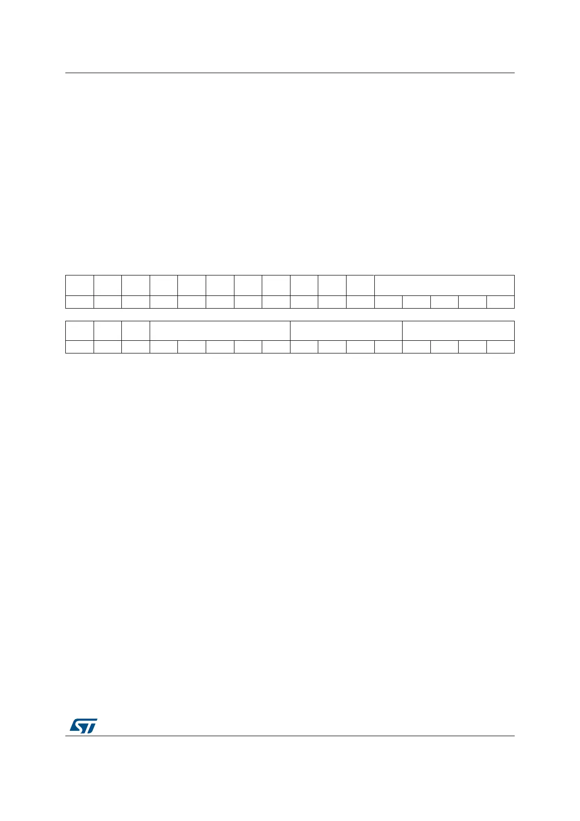
44.4.3 FDCAN data bit timing and prescaler register (FDCAN_DBTP)
Address offset: 0x000C
Reset value: 0x0000 0A33
This register is only writable if bits CCCR.CCE and CCCR.INIT are set. The CAN time
quantum may be programmed in the range of 1 to 32 FDCAN clock periods. tq = (DBRP + 1)
FDCAN clock period.
DTSEG1 is the sum of Prop_Seg and Phase_Seg1. DTSEG2 is Phase_Seg2. Therefore the
length of the bit time is (programmed values) [DTSEG1 + DTSEG2 + 3] tq or (functional
values) [Sync_Seg + Prop_Seg + Phase_Seg1 + Phase_Seg2] tq.
The Information Processing Time (IPT) is 0, meaning the data for the next bit is available at
the first clock edge after the sample point.
Note: With a FDCAN clock of 8 MHz, the value of 0x00300A33 configures the FDCAN for a fast bit
rate of 500 kbit/s.
31 30 29 28 27 26 25 24 23 22 21 20 19 18 17 16
Res. Res. Res. Res. Res. Res. Res. Res. TDC Res. Res. DBRP[4:0]
rw rw rw rw rw rw
1514131211109876543210
Res. Res. Res. DTSEG1[4:0] DTSEG2[3:0] DSJW[3:0]
rw rw rw rw rw rw rw rw rw rw rw rw rw
Bits 31:24 Reserved, must be kept at reset value.
Bit 23 TDC: Transceiver delay compensation
0: Transceiver delay compensation disabled
1: Transceiver delay compensation enabled
Bits 22:21 Reserved, must be kept at reset value.
Bits 20:16 DBRP[4:0]: Data bit rate prescaler
The value by which the oscillator frequency is divided to generate the bit time quanta. The bit
time is built up from a multiple of this quanta. Valid values for the Baud Rate Prescaler are 0
to 31. The hardware interpreters this value as the value programmed plus 1.
Bits 15:13 Reserved, must be kept at reset value.
Bits 12:8 DTSEG1[4:0]: Data time segment before sample point
Valid values are 0 to 31. The value used by the hardware is the one programmed,
incremented by 1, i.e. t
BS1
= (DTSEG1 + 1) x tq.
Bits 7:4 DTSEG2[3:0]: Data time segment after sample point
Valid values are 0 to 15. The value used by the hardware is the one programmed,
incremented by 1, i.e. t
BS2
= (DTSEG2 + 1) x tq.
Bits 3:0 DSJW[3:0]: Synchronization jump width
Must always be smaller than DTSEG2, valid values are 0 to 15. The value used by the
hardware is the one programmed, incremented by 1: t
SJW
= (DSJW + 1) x tq.
 Loading...


