Embedded Flash memory (FLASH) for category 2 devices RM0440
220/2126 RM0440 Rev 4
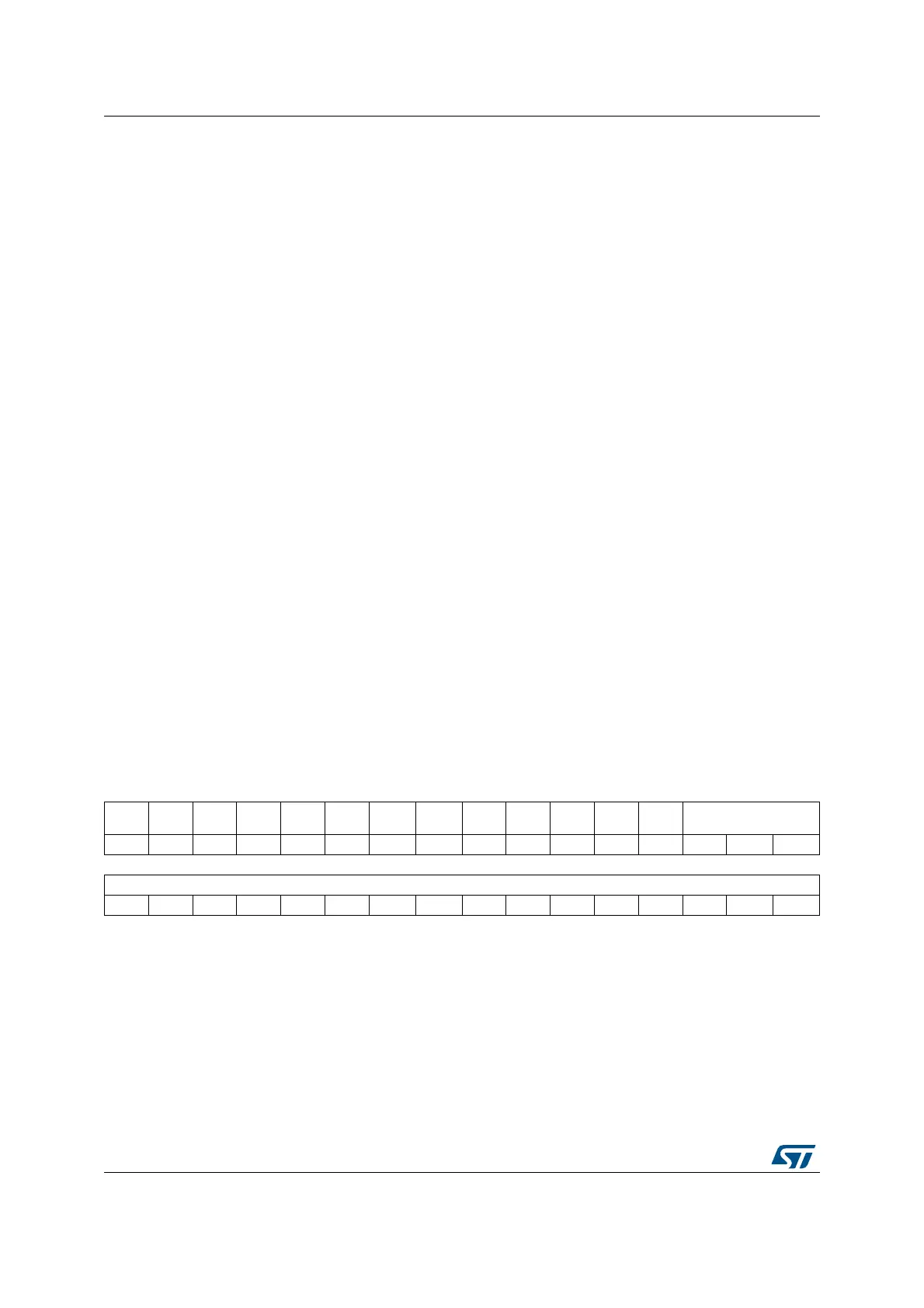
5.7.7 Flash ECC register (FLASH_ECCR)
Address offset: 0x18
Reset value: 0x0000 0000
Access: no wait state when no Flash memory operation is on going, word, half-word and
byte access
Bit 16 START: Start
This bit triggers an erase operation when set. If MER1, MER2 and PER bits are
reset and the STRT bit is set, an unpredictable behavior may occur without
generating any error flag. This condition should be forbidden.
This bit is set only by software, and is cleared when the BSY bit is cleared in
FLASH_SR.
Bits 15:11 Reserved, must be kept at reset value.
Bit 10 Reserved, must be kept at reset value.
Bits 9:3 PNB[6:0]: Page number selection
These bits select the page to erase:
00000000: page 0
00000001: page 1
...
11111111: page 255
Bit 2 MER1: Mass erase
This bit triggers the mass erase (all user pages) when set.
Bit 1 PER: Page erase
0: page erase disabled
1: page erase enabled
Bit 0 PG: Programming
0: Flash programming disabled
1: Flash programming enabled
31 30 29 28 27 26 25 24 23 22 21 20 19 18 17 16
ECCD ECCC Res. Res. Res. Res. Res.
ECCC
IE
Res.
SYSF_
ECC
Res. Res. Res. ADDR_ECC[18:16]
rc_w1 rc_w1 rw r r r r
1514131211109 8 765432 1 0
ADDR_ECC[15:0]
rrrrrr r r rrrrrr r r