True random number generator (RNG) RM0440
840/2126 RM0440 Rev 4
26.7 RNG registers
The RNG is associated with a control register, a data register and a status register.
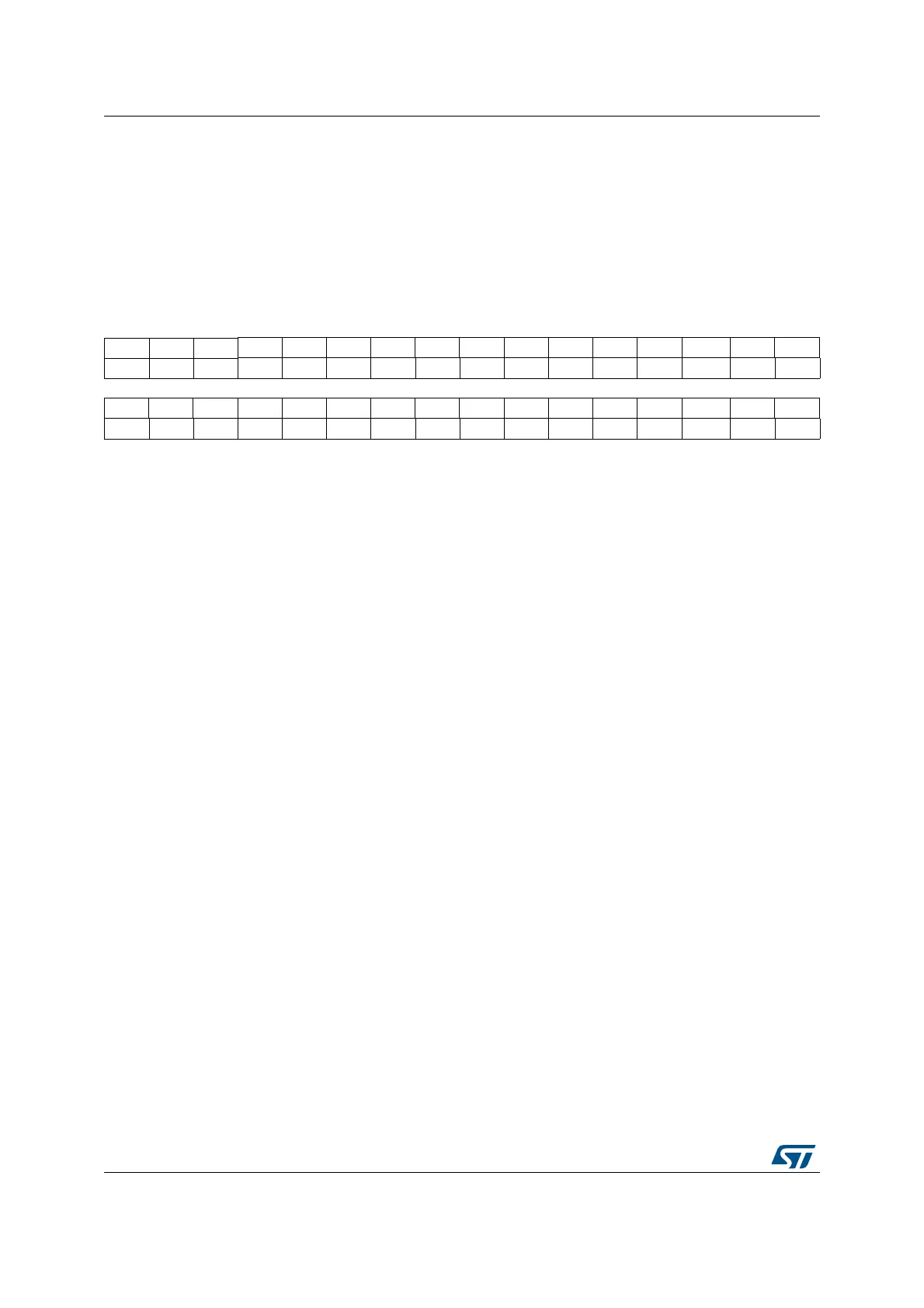
26.7.1 RNG control register (RNG_CR)
Address offset: 0x000
Reset value: 0x0000 0000
31 30 29 28 27 26 25 24 23 22 21 20 19 18 17 16
Res. Res. Res. Res. Res. Res. Res. Res. Res. Res. Res. Res. Res. Res. Res. Res.
15 14 13 12 11 10 9 8 7 6 5 4 3 2 1 0
Res. Res. Res. Res. Res. Res. Res. Res. Res. Res. CED Res. IE RNGEN Res. Res.
rw rw rw
Bits 31:6 Reserved, must be kept at reset value.
Bit 5 CED: Clock error detection
0: Clock error detection is enable
1: Clock error detection is disable
The clock error detection cannot be enabled nor disabled on-the-fly when the RNG is enabled,
i.e. to enable or disable CED the RNG must be disabled.
Bit 4 Reserved, must be kept at reset value.
Bit 3 IE: Interrupt Enable
0: RNG Interrupt is disabled
1: RNG Interrupt is enabled. An interrupt is pending as soon as DRDY=’1’, SEIS=’1’ or
CEIS=1 in the RNG_SR register.
Bit 2 RNGEN: True random number generator enable
0: True random number generator is disabled. Analog noise sources are powered off and
logic clocked by the RNG clock is gated.
1: True random number generator is enabled.
Bits 1:0 Reserved, must be kept at reset value.
 Loading...


