STC8A8K64D4 Series Manual
-
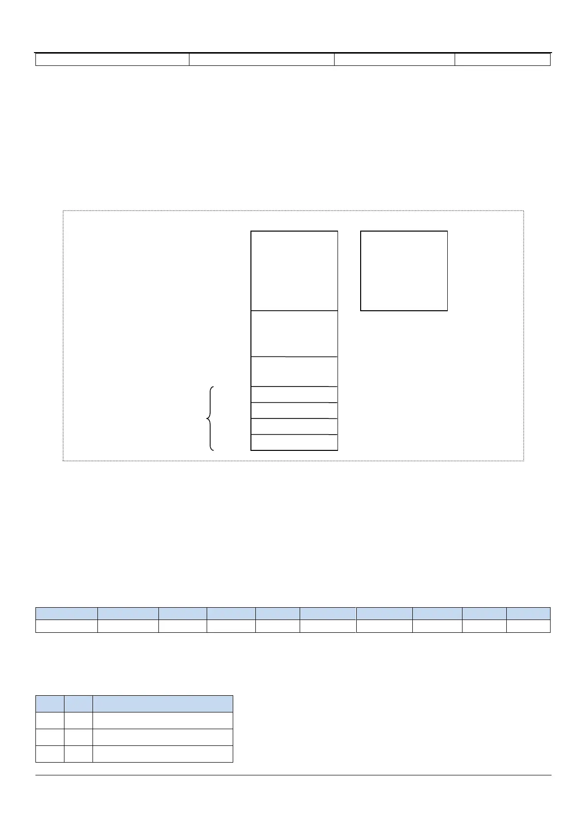
7.2.1 Internal RAM
A total of 256 bytes of internal RAM can be divided into two parts: Lower 128 bytes of RAM and Upper 128 bytes of
RAM. The Lower 128 bytes of data memory are compatible with the traditional 8051 microcontroller, which can be access
by either Direct addressing or Indirect addressing. The Upper 128 bytes of RAM (upper 128 bytes of RAM is extended in
8052) and special function registers, SFRs in short, occupy the same block of addresses, 80H to FFH, but they are physically
separate entities and are accessed using different addressing modes. Upper 128 bytes of RAM can only be accessed by Indirect
addressing, SFRs area can only be accessed by Direct addressing.
Internal RAM is mapped in the following figure.
The Lower 128 bytes of RAM are also called as general purpose RAM space. The general purpose RAM space can be
divided into working register banks space, bit addressable space, user RAM space and stack space. Total of 32 bytes of
working register bank space, 00H t0 1FH, are divided into 4 groups. Each group is called a register bank, which contains 8 8-
bit working registers. All the numbers in different register bank are R0 through R7, but they belong to different Physical space.
By using the working register registers, the operation speed can be increased. R0 ~ R7 are commonly used registers. Four
bank sare provided because one bank is often not enough. The combination of RS1 and RS0 in the PSW register determines
the working register bank currently used, see the introduction of PSW register below.
7.2.2 PSW (program status word register)
CY: Carry/borrow flag bit.
AC: Auxiliary carry/borrow flag bit.
F0: User flag bit 0
RS1, RS0: Working register select bit
working register bank (R0~R7)
Bit-addressable
Indirect
addressing
Direct
addressing
Register bank,
selected by RS0