can be considered as a 16-bit cyclic shift register. As data is shifted from the master to the slave, data is also shifted in
the opposite direction simultaneously. This means that the data of the master and the slave are exchanged with each
other in one shift period.
Change Mode using SS pin
If SPEN = 1, SSIG = 0 and MSTR = 1, SPI is enabled in master mode and the SS pin can be configured for input
mode or quasi-bidirectional port mode. In this case, another master can drive this pin low to select the device as an SPI
slave and send data to it. To avoid bus contention, the SPI system clears the slave’s MSTR, forces MOSI and SCLK to
be input mode, and MISO changes to output mode. The SPIF flag in SPSTAT is set, and if the SPI interrupt is enabled,
an SPI interrupt will occur.
The user software must always detect the MSTR bit. If this bit is cleared by a slave selection action and the user
wants to continue using the SPI as a master, the MSTR bit must be set again, otherwise it will remain in slave mode.
Write Collision
The SPI is single buffered in the transmition process and double buffered in receiving process. New data for
transmission can not be written to the shift register until the previous transmission is complete. The WCOL bit will be
set to indicate that a data write collision error has occurred when the data register SPDAT is written during transmission.
In this case, the data currently being transmitted will continue to be transmitted, and the newly written data will be lost.
A write collision condition on the master is rare when write collision detection is performed on a master or slave
because the master has full control of the data transfer. However, a write collision may occur on the slave because the
slave can not control it when the master initiates the transfer.
When receiving data, the received data is transferred to a parallel read data buffer, which will release the shift
register for the next data reception. However, the received data must be read from the data register before the next
character is completely shifted in. Otherwise, the previous received data will be lost.
WCOL can be cleared by software by writing “1” to it.
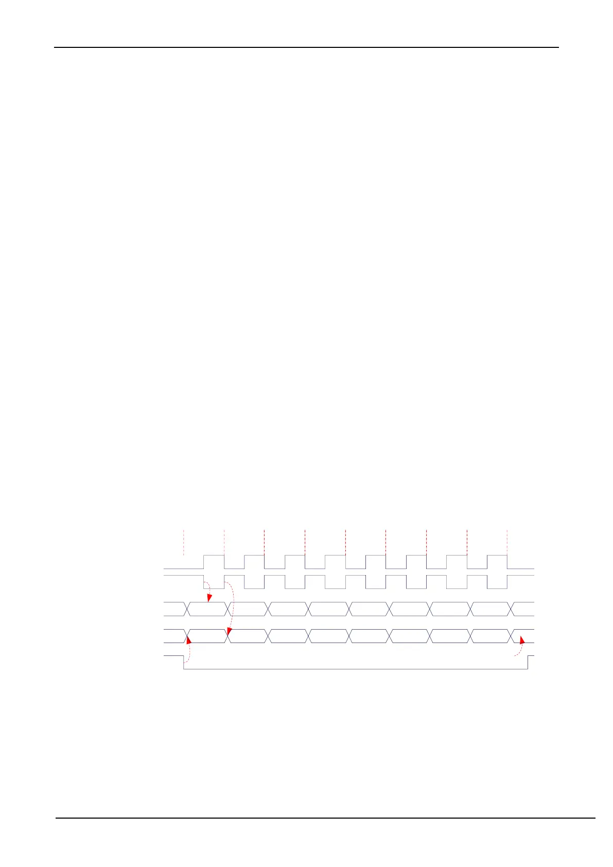
20.5 Data Format
The clock phase control bit, CPHA, of the SPI allows the user to set the clock edge when the data is sampled and
changed. The clock polarity bit, CPOL, allows the user to set the clock polarity. The following illustrations show the
SPI communication timing under different clock phases and polarity settings.