EasyManua.ls Logo

STC micro STC8A8K64D4 Series - Function Pins Switch; Register Related to Function Pin Switch; Bus Speed Control Register (BUS_SPEED); Peripheral Port Switch Register 1(P_SW1) (for UART1, CCP, SPI Switching)

Default Icon
901 pages
Print Icon
To Next Page IconTo Next Page
To Previous Page IconTo Previous Page
Loading...
STC8A8K64D4 Series Manual
-
- 15 -
3 Function pins switch
Some special peripherals of STC8A8K64D4 series of microcontrollers can be switched among several I/O pins to realize
one peripheral used as multiple device through time-sharing, such as UART, SPI, PCA, I2C and bus control pins.
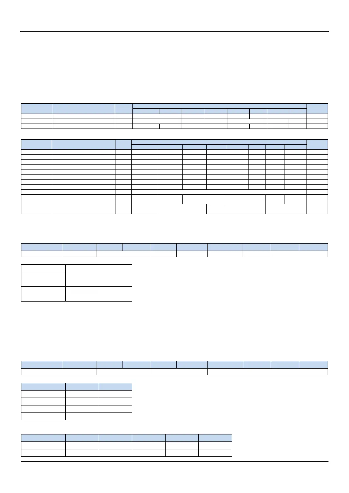
3.1 Register related to function pin switch
Symbol
Description
Address
Bit Address and Symbol
Reset
value
B7
B6
B5
B4
B3
B2
B1
B0
BUS_SPEED
Bus speed control register
A1H
RW_S[1:0]
SPEED[1:0]
00xx,xx00
P_SW1
Peripheral port switch register 1
A2H
S1_S[1:0]
CCP_S[1:0]
SPI_S[1:0]
0
-
nn00,000x
P_SW2
Peripheral port switch register 2
BAH
EAXFR
I2C_S[1:0]
CMPO_S
S4_S
S3_S
S2_S
0x00,0000
Symbol
Description
Address
Bit Address and Symbol
Reset
value
B7
B6
B5
B4
B3
B2
B1
B0
PWM0CR
PWM0 Control register
FF14H
ENC0O
C0INI
-
C0_S[1:0]
EC0I
EC0T2SI
EC0T1SI
00x0,0000
PWM1CR
PWM1 Control register
FF1CH
ENC1O
C1INI
-
C1_S[1:0]
EC1I
EC1T2SI
EC1T1SI
00x0,0000
PWM2CR
PWM2 Control register
FF24H
ENC2O
C2INI
-
C2_S[1:0]
EC2I
EC2T2SI
EC2T1SI
00x0,0000
PWM3CR
PWM3 Control register
FF2CH
ENC3O
C3INI
-
C3_S[1:0]
EC3I
EC3T2SI
EC3T1SI
00x0,0000
PWM4CR
PWM4 Control register
FF34H
ENC4O
C4INI
-
C4_S[1:0]
EC4I
EC4T2SI
EC4T1SI
00x0,0000
PWM5CR
PWM5 Control register
FF3CH
ENC5O
C5INI
-
C5_S[1:0]
EC5I
EC5T2SI
EC5T1SI
00x0,0000
PWM6CR
PWM6 Control register
FF44H
ENC6O
C6INI
-
C6_S[1:0]
EC6I
EC6T2SI
EC6T1SI
00x0,0000
PWM7CR
PWM7 Control register
FF4CH
ENC7O
C7INI
-
C7_S[1:0]
EC7I
EC7T2SI
EC7T1SI
00x0,0000
MCLKOCR
Master clock output control register
FE05H
MCLKO_S
MCLKODIV[6:0]
0000,0000
LCMIFCFG
LCM Interface Configuration
Register
FE50H
LCMIFIE
-
LCMIFIP[1:0]
LCMIFPS[1:0]
D16_D8
M68_80
0x00,0000
LCMIFCFG2
LCM Interface Configuration
Register 2
FE51H
LCMIFEXPS[1:0]
SETUPT[2:0]
HOLDT[1:0]
x000,0000
3.1.1 Bus Speed Control Register (BUS_SPEED)
Symbol
Address
B7
B6
B5
B4
B3
B2
B1
B0
BUS_SPEED
A1H
RW_S[1:0]
SPEED[1:0]
RW_S[1:0]: External bus RD/WR control line select bits
RW_S[1:0]
RD
WR
00
P4.4
P4.3
01
P3.7
P3.6
10
P4.2
P4.0
11
Reserved
3.1.2 Peripheral port switch register 1(P_SW1) (for UART1, CCP, SPI
switching)
Symbol
Address
B7
B6
B5
B4
B3
B2
B1
B0
P_SW1
A2H
S1_S[1:0]
CCP_S[1:0]
SPI_S[1:0]
0
-
S1_S[1:0]USART1 pin selection bits
S1_S[1:0]
RxD
TxD
00
P3.0
P3.1
01
P3.6
P3.7
10
P1.6
P1.7
11
P4.3
P4.4
CCP_S[1:0]: PCA pin selection bits
CCP_S[1:0]
ECI
CCP0
CCP1
CCP2
CCP3
00
P1.2
P1.7
P1.6
P1.5
P1.4
01
P2.2
P2.3
P2.4
P2.5
P2.6

Table of Contents

Related product manuals