STC8A8K64D4 Series Manual
-
7.2.6 Bus speed control register (BUS_SPEED)
RW_S[1:0]: RD/WR control line selection bit
00: P4.4 is RD, P4.3 is WR
01: P3.7 is RDP3.6 is WR
10: P4.2 is RDP4.0 is WR
11: Reserved.
SPEED[2:0]: Bus read and write speed control (preparation time and hold time of control signal and data signal when reading
and writing data)
Access internal expansion RAM
Access external expansion RAM
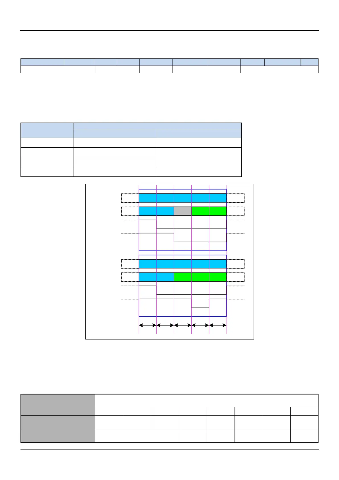
The timing of reading and writing external extended RAM is shown in the figure below:
Writing to External Expansion RAM
P2 (A[15:8])
P0 (AD[7:0])
P4.1 (ALE)
P4.4 (RD)
P2 (A[15:8])
P0 (AD[7:0])
P4.1 (ALE)
P4.3 (WR)
High 8-bit address
Lower 8-bit address Data Of being read
High 8-bit address
Lower 8-bit address Data to be written
setup
ADRL
hold
ADRL
setup
DAT
Read
Write
hold
DAT
Read external extended RAM
7.2.7 Bit Addressable Data Memory in 8051
Bit addressable data memory integrated in 8051 single-chip includes two parts: the address range of the first part is 00H ~ 7FH,
and the address range of the second part is 80H ~ FFH. The 00H ~ 7FH bit addressing area is a mapping of the 16 bytes of the data
area 20H ~ 2FH, and the 80H ~ FFh bit addressing area is the 16 special function registers whose addresses are divisible by 8.
(Including 80H, 88H, 90H, 98H, A0H, A8H, B0H, B8H, C0H, C8H, D0H, D8H, E0H, E8H, F0H, F8H).
Address of Bit-addressable