STC8A8K64D4 Series Manual
it still needs To enable the ADC channel, you need to set the PxIE register to close the digital input channel
to prevent the external analog input signal from fluctuating high and low and causing additional power
consumption)
17.1.2 ADC configuration register (ADCCFG)
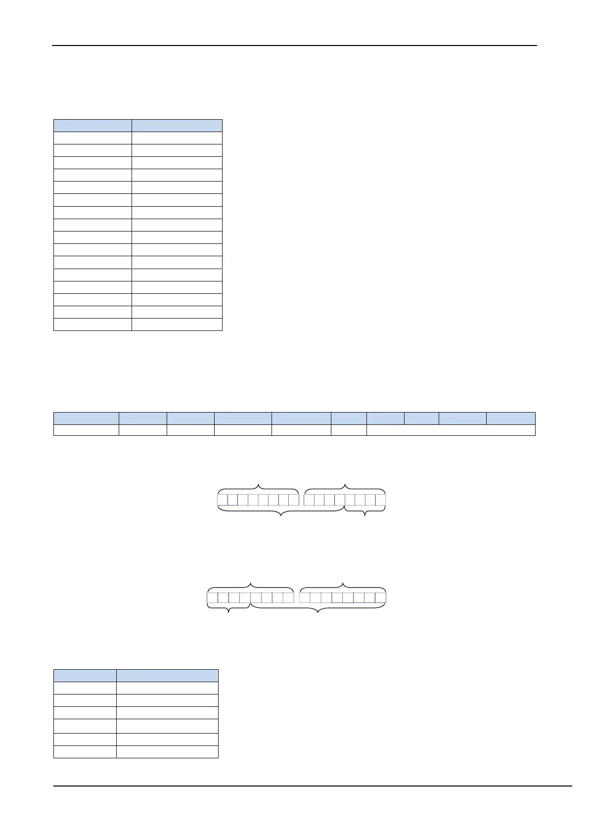
RESFMT: ADC conversion result format control bit
0: The conversion result aligns left. ADC_RES is used to save the upper 8 bits of the result and ADC_RESL is
used to save the lower 4 bits of the result. The format is as follows:
RESFMT=0
ADC_RES ADC_RESL
D9 D8 D7 D6 D5 D4 D3 D2 D1 D0
D11 D10
0 0 0 0
12 bit conversion result Fill 0 automatically
1: The conversion result aligns right. ADC_RES is used to save the upper 4 bits of the result and ADC_RESL is
used to save the lower 8 bits of the result. The format is as follows:
RESFMT=1
ADC_RES ADC_RESL
D7 D6 D5 D4 D3 D2 D1 D00 0 0 0 D11 D10 D9 D8
12 bit conversion resultFill 0 automatically
SPEED[3:0]: ADC clock control bits {F
ADC
=SYSclk/2/(SPEED+1)}