STC8A8K64D4 Series Manual
-
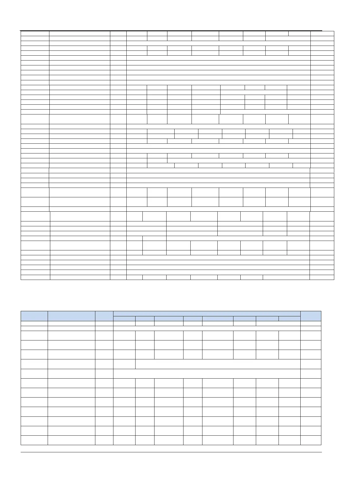
Program Status Word Register
Timer4 and Timer 3 Control Register
Timer 4 high byte register
Timer 4 low byte register
Timer 3 high byte register
Timer 3 low byte register
Timer 2 high byte register
Timer 2 low byte register
PCA Module 0 Control Register
PCA Module 1 Control Register
PCA Module 2 Control Register
ADC Configuration Register
3nd Interrupt Priority register low
byte
2nd Data pointer low byte
2nd Data pointer high byte
Comparator Control Register 1
Comparator Control Register 2
3nd Interrupt Priority Register High
Byte
Extended External Interrupt Flag
Register
Enhanced PWM global
configuration
PWM mode register of PCA0
PWM mode register of PCA1
PWM mode register of PCA2
IAP Waiting Time Control Register
Enhanced PWM Configuration
Register
Reset Configuration Register
The following special function registers are extended SFRs whose logical addresses are in the XDATA area. Before
access them, the highest bit (EAXFR) of the P_SW2 (BAH) register needs to be set, and they can accessed by using the
MOVX A, @DPTR and MOVX @ DPTR, A instructions.
Internal high-speed
oscillator Control Register
External Oscillator Control
Register
Internal 32K Oscillator
Control Register
Main Clock Output Control
Register
Internal high-speed
oscillator debounce control
P0 Pull-up Resistor Control
Register
P1 Pull-up Resistor Control
Register
P2 Pull-up Resistor Control
Register
P3 Pull-up Resistor Control
Register
P4 Pull-up Resistor Control
Register
P5 Pull-up Resistor Control
Register
P6 Pull-up Resistor Control
Register