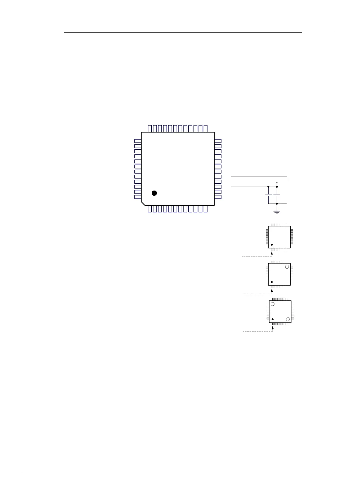
LQFP48
QFN48
RxD4_2/P5.2 1
TxD4_2/P5.3 2
TxD2/PWM1_2/ADC1/P1.1 3
ADC_ETR/ECI/T2/SS/PWM2_2/ADC2/P1.2 4
T2CLKO/MOSI/PWM3_2/ADC3/P1.3 5
CCP3/I2CSDA/MISO/PWM4_2/ADC4/P1.4 6
TxD_4/RD/P4.4 7
CCP2/I2CSCL/SCLK/PWM5_2/ADC5/P1.5 8
XTALO/CCP1/MCLKO_2/PWM6_2/RxD_3/ADC6/P1.6 9
XTALI/CCP0/PWM7_2/TxD_3/ADC7/P1.7 10
ADC_AGnd 11
AVref 12
CCP3_2/PWM6/A14/P2.6 37
PWM7/A15/P2.7 38
RxD3/ADC8/AD0/P0.0 39
TxD3/ADC9/AD1/P0.1 40
RxD4/ADC10/AD2/P0.2 41
RxD_4/WR/P4.3 42
TxD4/ADC11/AD3/P0.3 43
T3/ADC12/AD4/P0.4 44
T3CLKO/ADC13/AD5/P0.5 45
T4/ADC14/AD6/P0.6 46
T4CLKO/AD7/P0.7 47
RxD2/PWM0_2/ADC0/P1.0 48
36 P2.5/A13/PWM5/SCLK_2/CCP2_2/I2CSCL_2
35 P2.4/A12/PWM4/MISO_2/CCP1_2/I2CSDA_2
34 P2.3/A11/PWM3/MOSI_2/CCP0_2
33 P2.2/A10/PWM2/SS_2/ECI_2
32 P2.1/A9/PWM1
31 P4.2/RD_3/TxD2_2
30 P2.0/A8/PWM0/RSTSV
29 P4.1/ALE/CMPO_2
28 P3.7/INT3/RD_2/TxD_2/CMP+
27 P3.6/INT2/WR_2/RxD_2/CMP-
26 P5.1/TxD3_2/CMP+_3
25 P5.0/RxD3_2/CMP+_2
24 P3.5/T1/T0CLKO/ECI_4/SS_4/PWMFLT
23 P3.4/T0/T1CLKO/MOSI_4/CMPO
22 P3.3/INT1/CCP0_4/MISO_4/I2CSDA_4
21 P3.2/INT0/CCP1_4/SCLK_4/I2CSCL_4
20 P3.1/TxD/CCP2_4
19 P3.0/RxD/CCP3_4/INT4
18 P4.0/WR_3/RxD2_2
17 Gnd
16 P5.5
15 Vcc
14 P5.4/NRST/MCLKO
13 ADC_AVcc
Note:
If USB download is not required,
P3.0/P3.1/P3.2 cannot be low at the
same time when the chip is reset,
otherwise, the chip will always be
in USB download mode without
running user code.
0.1u22u
MCU-VCC
1
st
pin
1
st
pin
1
st
pin
STC
STC
STC
Looking at the chip silk screen, the small dot at the
bottom left is the first Pin.
Looking at the chip silkscreen, the last letter
of the bottom line is the chip version number