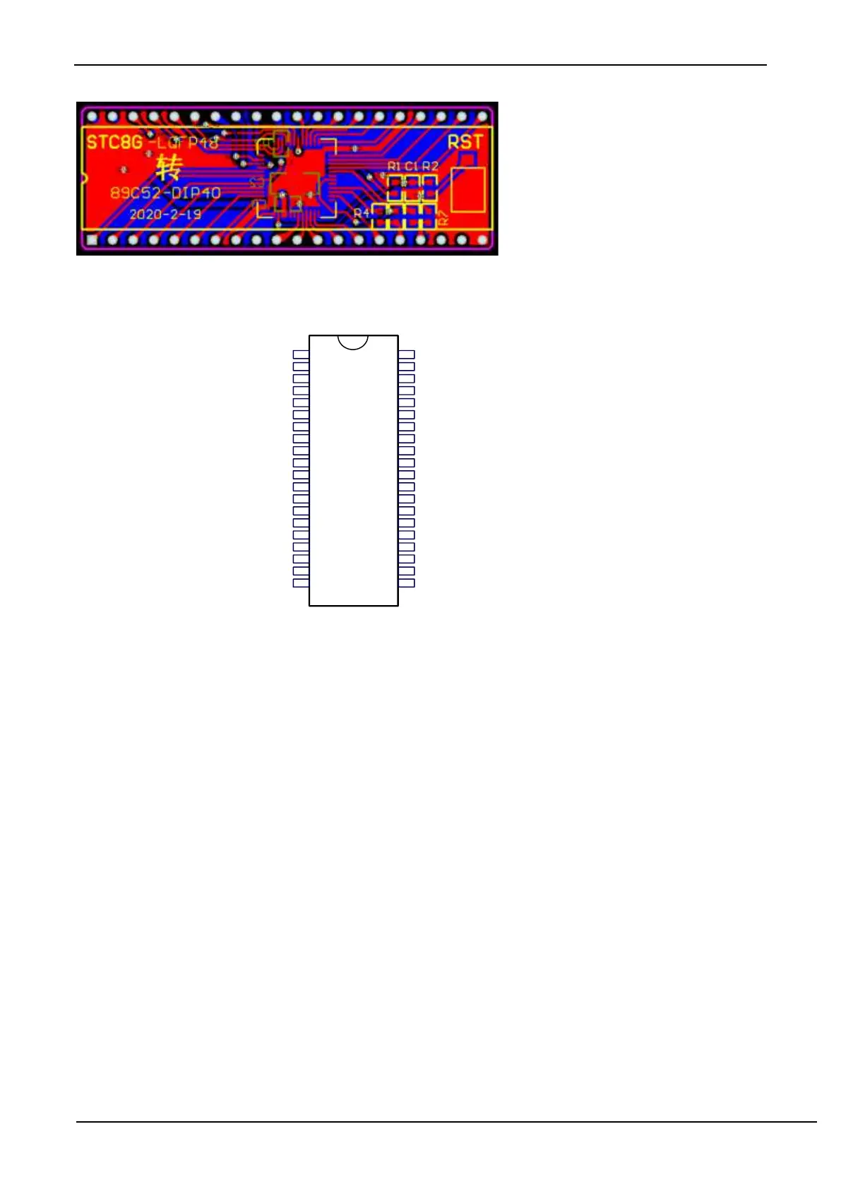
STC8G2K64S4 - LQFP48
To
STC89C52RC – PDIP40
RxD3/AD0/ADC8/PWM00/P0.0 1
TxD3/AD1/ADC9/PWM01/P0.1 2
RxD4/AD2/ADC10/PWM02/P0.2 3
TxD4/AD3/ADC11/PWM03/P0.3 4
T3/AD4/ADC12/PWM04/P0.4 5
T3CLKO/AD5/ADC13/PWM05/P0.5 6
PWMFLT2/T4/AD6/ADC14/PWM06/P0.6 7
PWMFLT3/T4CLKO/AD7/PWM07/P0.7 8
RST(NC) 9
INT4/RxD/PWM30/P3.0 10
TxD/PWM31/P3.1 11
I2CSCL_4/SCLK_4/INT0/PWM32/P3.2 12
I2CSDA_4/MISO_4/INT1/PWM33/P3.3 13
CMPO/MOSI_4/ECI_2/T1CLKO/T0/PWM34/P3.4 14
PWMFLT/CCP0_2/SS_4/T0CLKO/T1/PWM35/P3.5 15
CCP1_2/CMP-/RxD_2/INT2/PWM36/P3.6 16
/CCP2/CCP2_2/CMP+TxD_2/INT3/PWM37/P3.7 17
XTAL2(NC) 18
XTAL1(NC) 19
GND 20
40 VCC
39 P0.0/PWM00/ADC8/AD0/RxD3
38 P0.1/PWM01/ADC9/AD1/TxD3
37 P0.2/PWM02/ADC10/AD2/RxD4
36 P0.3/PWM03/ADC11/AD3/TxD4
35 P0.4/PWM04/ADC12/AD4/T3
34 P0.5/PWM05/ADC13/AD5/T3CLKO
33 P0.6/PWM06/ADC14/AD6/T4/PWMFLT2
32 P0.7/PWM07/AD7/T4CLKO/PWMFLT3
31 EA(P4.7/PWM47/TxD2_2)
30 ALE(P4.5/PWM45)
29 PSEN(P4.6/PWM46/RD/RxD2_2)
28 P2.7/PWM27/A15/CCP2_3
27 P2.6/PWM26/A14/CCP1_3
26 P2.5//PWM25/A13/CCP0_3/I2CSCL_2/SCLK_2
25 P2.4/PWM24/A12/ECI_3/I2CSDA_2/MISO_2
24 P2.3/PWM23/A11/MOSI_2
23 P2.2/PWM22/A10/SS_2
22 P2.1/PWM21/A9
21 P2.0/PWM20/A8
Note:
✓ Due to the built-in high-precision R/C clock, no external crystal is needed, XTAL1 and XTAL2 can be empty.
✓ WR and RD are P4.2/ WR and P4.4/ RD respectively, not traditional WR/P3.6 and RD/P3.7.
(In the conversion board, P4.2 and P3.6 are connected together, and P4.4 and P3.7 are connected together.
When this conversion board is used to access the external bus, P3.6 and P3.7 should be set to high-
impedance input mode, so that P4.2 and P4.4 can normally output the bus read and write signals. If the
external bus is not needed to be accessed, P4.2 and P4.4 should be set to high-impedance input mode, and
P3.6 and P3.7 are ordinary I/O.)
✓ The STC8A8K64D4 series MCUs are low-level reset, it is not compatible with the high-level reset of the
traditional 8051, so the RST pin is left floating, and replaced by the reset button and reset circuit on the conversion
board.