17
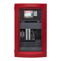
Figure 1-1. Standalone 4100ES System.............................................................................. 1-3
Figure 1-2. MINIPLEX 4100ES System.............................................................................. 1-5
Figure 1-3. Hub/Ring Configuration .................................................................................... 1-6
Figure 1-4. Interconnected Loop Configuration................................................................... 1-7
Figure 2-1. The CPU Bay..................................................................................................... 2-2
Figure 2-2. Master Motherboard (566-227)......................................................................... 2-3
Figure 2-3. Master Controller Daughter Card (566-719)..................................................... 2-4
Figure 2-4. System Power Supply (566-071)...................................................................... 2-6
Figure 2-5. The Power Distribution Interface (PDI)............................................................. 2-7
Figure 2-6. RUI+ CPU Master Motherboard (566-938)....................................................... 2-7
Figure 2-7. Master Controller Daughter Card (566-719)..................................................... 2-8
Figure 2-8. EPS with IDNet 2 (566-872) ........................................................................... 2-10
Figure 2-9. IDNet 2 Card................................................................................................... 2-11
Figure 2-10. Operator Interface......................................................................................... 2-12
Figure 2-11. Flexible User Interface.................................................................................. 2-12
Figure 2-12. Expansion Bays............................................................................................ 2-13
Figure 2-13. System Power............................................................................................... 2-14
Figure 2-14. Back Box Installation Diagram...................................................................... 2-16
Figure 2-15. Back Box side views (plastic and metal doors).............................................. 2-17
Figure 2-16. Removing the Shipping Studs ...................................................................... 2-18
Figure 2-17. Mounting the PDM Bracket (2-Bay Box Shown)........................................... 2-19
Figure 2-18. Installing the System Electronics Bay Assembly .......................................... 2-20
Figure 2-19. Semi-Flush Trim Kit ...................................................................................... 2-21
Figure 2-20. Applying the Trim.......................................................................................... 2-21
Figure 2-21. Front and Back View of a Glass Door........................................................... 2-22
Figure 2-22. Front and Back view of a Solid Door ............................................................ 2-22
Figure 2-23. Reversing the Lock Catch............................................................................. 2-23
Figure 2-24. Securing the Dress Panel............................................................................. 2-23
Figure 2-25. Hinge Pin Alignment ..................................................................................... 2-23
Figure 2-26. The Ground Wire .......................................................................................... 2-24
Figure 2-27. CPU Bay Card Placement............................................................................ 2-25
Figure 2-28. Expansion Bay 4” X 5” Card Placement ....................................................... 2-26
Figure 2-29. Expansion Bay Motherboard Placement ...................................................... 2-27
Figure 2-30. Mixed Module Placement ............................................................................. 2-28
Figure 2-31. Slave Card/PDI Connection.......................................................................... 2-29
Figure 2-32. Installing the Motherboard in a 4100ES Expansion Bay............................... 2-30
Figure 2-33. Wiring Looped Through Ferrite Bead ........................................................... 2-31
Figure 2-34. FACP Power Supply Assembly Connector (EPS shown)............................. 2-32
Figure 2-35. XPS/PDM Connection .................................................................................. 2-33
Figure 2-36. Bay-to-Bay Interconnections......................................................................... 2-34
Figure 2-37. Basic CPU Interconnections......................................................................... 2-37
Figure 2-38. Power and Communication Wiring for Motherboards................................... 2-38
Figure 2-39. One Bay Battery Installation......................................................................... 2-41
Figure 2-40. Multi-Bay Battery Installation........................................................................ 2-42
Figure 2-41. Terminal Block Utility Module Mounting........................................................ 2-44
Figure 3-1. Transponder Interface Cards............................................................................. 3-4
Figure 3-2. TIC Mounting .................................................................................................... 3-9
Figure 3-3. Transponder Cabinet Interconnections........................................................... 3-10
Figure 3-4. Loop Wire Through Ferrite Bead as Shown ................................................... 3-11
Figure 3-5. TIC Wiring to the Host Panel .......................................................................... 3-11
Figure 3-6. Analog Audio Interconnections....................................................................... 3-12
Figure 3-7. Digital Interconnections (4100-1311 Digital Audio Controller)........................ 3-13
Figure 4-1. 4100-6014 Network Interface Card.................................................................... 4-3
Figure 4-2. UT Motherboard with City Connection (565-274) ............................................. 4-4
Figure 4-3. UT Motherboard without City Connection (565-275) ........................................ 4-4
Figure 4-4. The 4100/4120-0143/ 4100-6057 Fiber-Optic Media Card............................... 4-5
Figure 4-5. The 4100/4120-0142 Wired Media Card (565-413).......................................... 4-5
Figure 4-6. The 4100-6055 Modem Media Card (565-279 or 566-338).............................. 4-6
Figure 4-7. Media Card Mounting ....................................................................................... 4-9
Figure 4-8. Installing the Daughter Card........................................................................... 4-10
Figure 4-9. The Transient Suppressor .............................................................................. 4-12
Figure 4-10. Fiber Wiring .................................................................................................. 4-13
Figure 4-11. Coupler Wiring.............................................................................................. 4-15
List of Figures