RM0440 Rev 4 1113/2126
RM0440 Advanced-control timers (TIM1/TIM8/TIM20)
1226
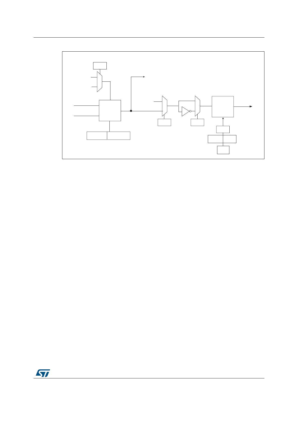
Figure 299. Output stage of capture/compare channel (channel 5, idem ch. 6)
1. Not available externally.
The capture/compare block is made of one preload register and one shadow register. Write
and read always access the preload register.
In capture mode, captures are actually done in the shadow register, which is copied into the
preload register.
In compare mode, the content of the preload register is copied into the shadow register
which is compared to the counter.
28.3.9 Input capture mode
In Input capture mode, the capture/compare Registers (TIMx_CCRx) are used to latch the
value of the counter after a transition detected by the corresponding ICx signal. When a
capture occurs, the corresponding CCXIF flag (TIMx_SR register) is set and an interrupt or
a DMA request can be sent if they are enabled. If a capture occurs while the CCxIF flag was
already high, then the over-capture flag CCxOF (TIMx_SR register) is set. CCxIF can be
cleared by software by writing it to ‘0’ or by reading the captured data stored in the
TIMx_CCRx register. CCxOF is cleared when it is written with 0.
The following example shows how to capture the counter value in TIMx_CCR1 when tim_ti1
input rises. To do this, use the following procedure:
• Select the active input: TIMx_CCR1 must be linked to the tim_ti1 input, so write the
CC1S bits to 01 in the TIMx_CCMR1 register. As soon as CC1S becomes different
from 00, the channel is configured in input and the TIMx_CCR1 register becomes read-
only.
• Program the appropriate input filter duration in relation with the signal connected to the
timer (when the input is one of the tim_tix (ICxF bits in the TIMx_CCMRx register). Let’s
imagine that, when toggling, the input signal is not stable during at must 5 internal clock
cycles. We must program a filter duration longer than these 5 clock cycles. We can
validate a transition on tim_ti1 when 8 consecutive samples with the new level have
MSv62324V3
Output
mode
controller
CNT > CCR5
CNT = CCR5
TIMx_CCMR3
OC5M[3:0]
0
1
CC5P
TIMx_CCER
Output
enable
circuit
tim_oc5
CC5E
TIMx_CCER
To the master
mode controller
tim_oc5ref
OC5CE
0
1
CC5E
TIMx_CCER
‘0’
TIMx_BDTR
OSSI
MOE
OIS5
TIMx_CR2
(1)
0
1
ocref_clr_int
tim_etrf
tim_ocref_clr
OCCS
TIMx_SMCR
 Loading...


