RM0440 Rev 4 1229/2126
RM0440 General-purpose timers (TIM2/TIM3/TIM4/TIM5)
1343
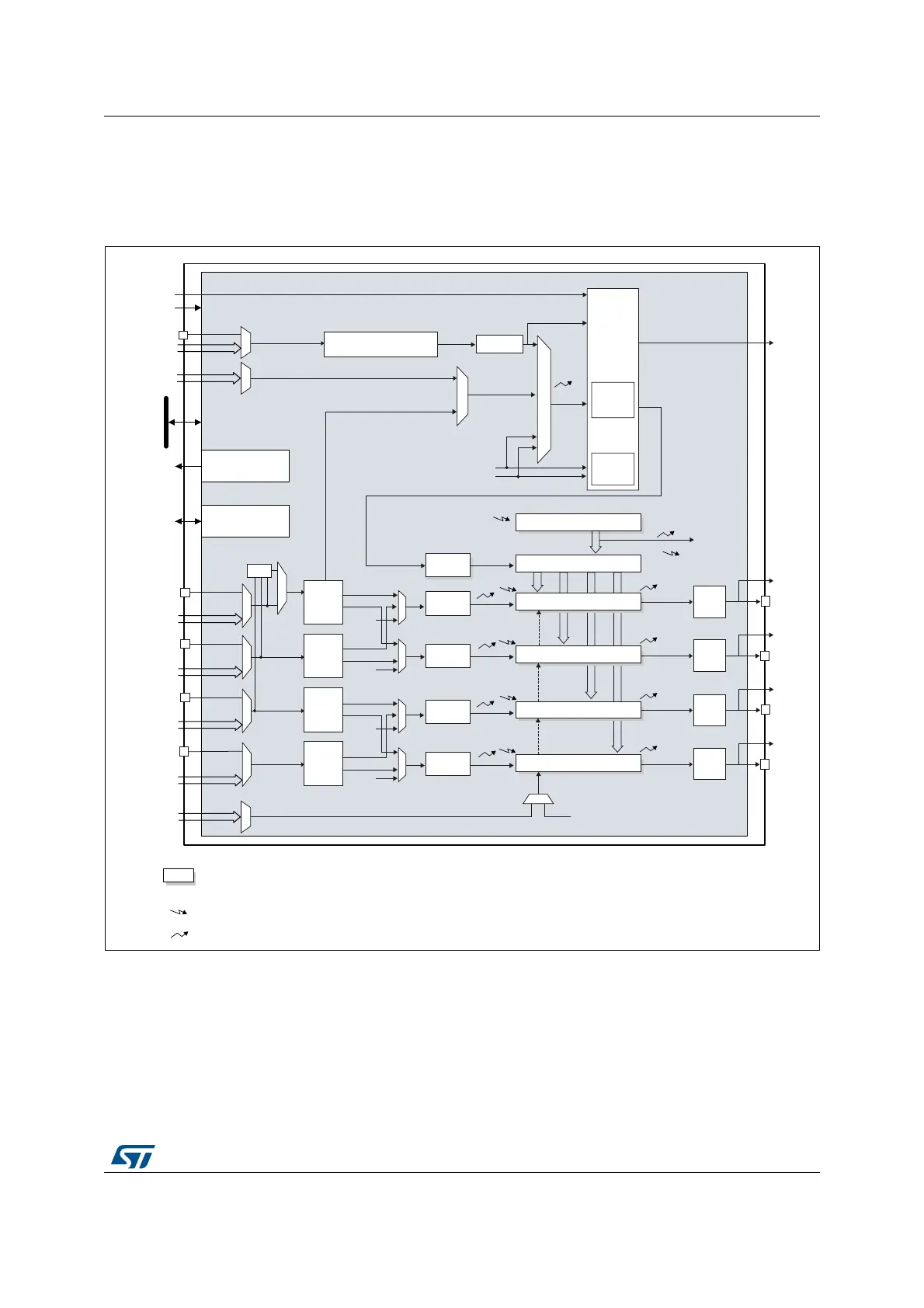
29.4 TIM2/TIM3/TIM4/TIM5 functional description
29.4.1 Block diagram
Figure 358. General-purpose timer block diagram
1. This feature is not available on all timers, refer to the Section 29.3: TIM2/TIM3/TIM4/TIM5 implementation.
MSv62373V2
U
U
U
CC1I
CC2I
Trigger
controller
+/-
Stop, clear or up/down
Output
control
U
UI
Reset
enable
up/down
count
TRG
CC1I
CC2I
TIM_CH2
TIM_CH1
PSC
prescaler
CNT counter
Capture/Compare 1 register
Notes:
Reg
Preload registers transferred
to active registers on U event
according to control bit
Event
Interrupt & DMA output
Auto-reload register
Capture/Compare 2 register
Prescaler
Prescaler
Output
control
U
U
CC3I
CC4I
Output
control
TIM_CH4
TIM_CH3
Capture/Compare 3 register
Capture/Compare 4 register
Prescaler
Prescaler
Output
control
CC3I
CC4I
Encoder
interface
Input filter
Polarity selection & edge
detector & prescaler
tim_etrf
tim_itr[15..0]
TIM_CH1
XOR
Input
filter &
edge
detector
Input
filter &
edge
detector
Input
filter &
edge
detector
Input
filter &
edge
detector
TIM_CH2
TIM_CH3
TIM_CH4
tim_ti4
tim_ti3
tim_ti2
tim_ti1
tim_ti1fp1
tim_trc
tim_trc
tim_trc
tim_trc
tim_ti1fp2
tim_ti2fp1
tim_ti2fp2
tim_ti3fp3
tim_ti3fp4
tim_ti4fp3
tim_ti4fp4
tim_ic1
tim_ic2
tim_ic3
tim_ic4
tim_psc_ck tim_cnt_ck
tim_ti1fp1
tim_ti2fp2
tim_trc
tim_ti1f_ed
tim_itr
tim_etrp
tim_etrf
tim_trgi
tim_etr_in
tim_ker_ck
tim_oc1ref
tim_oc2ref
tim_oc3ref
tim_oc4ref
tim_oc1
tim_oc2
tim_oc3
tim_oc4
Slave
controller
mode
tim_trgo
TIM_ETR
tim_etr[15:1]
tim_etr0
DMA interface
IRQ interface
tim_pclk
32-bit APB
bus
tim_cc1_dma
tim_cc2_dma
tim_cc3_dma
tim_cc4_dma
tim_upd_dma
tim_trg_dma
tim_com_dma
tim__it
tim_ti4_in[15:1]
tim_ti1_in0
tim_ti1_in1
tim_ti1_in2
tim_ti1_in3
tim_ti3_in[15:1]
tim_ti2_in[15:1]
tim_ti1_in[15:1]
tim_ocref_clr [7..0]
(1)
tim_ocref_clr
(1)
tim_ocref_clr_int
 Loading...


