Embedded Flash memory (FLASH) for category 4 devices RM0440
180/2126 RM0440 Rev 4
4.7.8 Flash option register (FLASH_OPTR)
Address offset: 0x20
Reset value: 0xFXXX XXXX. Register bits are loaded with values from Flash memory at
OBL.
Access: no wait state when no Flash memory operation is on going, word, half-word and
byte access
Bit 24 ECCCIE: ECC correction interrupt enable
0: ECCC interrupt disabled
1: ECCC interrupt enabled.
This bit enables the interrupt generation when the ECCC bit in the FLASH_ECCR
register is set.
Bit 23 Reserved, must be kept at reset value.
Bit 22 SYSF_ECC: System Flash ECC fail
This bit indicates that the ECC error correction or double ECC error detection is
located in the System Flash.
Bits 21:19 Reserved, must be kept at reset value.
Bits 18:0 ADDR_ECC: ECC fail address
This bit indicates which address in the Flash memory is concerned by the ECC
error correction or by the double ECC error detection.
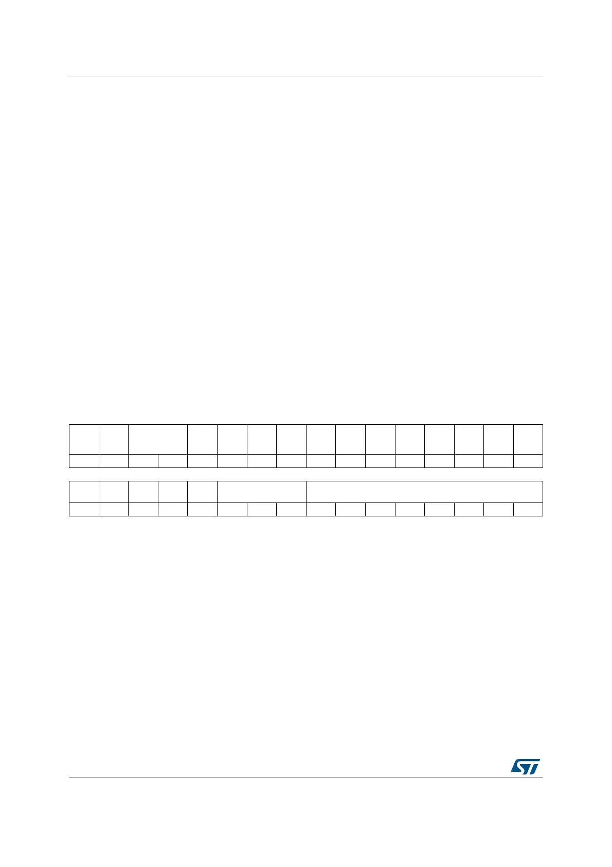
31 30 29 28 27 26 25 24 23 22 21 20 19 18 17 16
Res. IRHEN
NRST_MODE
[1:0]
n
BOOT0
nSW
BOOT0
CCM
SRAM_
RST
SRAM
_PE
nBOOT
1
PB4_P
UPEN
Res. Res.
WWDG
_SW
IWGD_
STDBY
IWDG_
StOP
IWDG_
SW
rw rw rw rw rw rw rw rw rw rw rw rw rw
1514131211109876543210
Res.
nRST_
SHDW
nRST_
STDBY
nRST_
STOP
Res. BOR_LEV[2:0] RDP[7:0]
rw rw rw rw rw rw rw rw rw rw rw rw rw rw
Bit 31 Reserved, must be kept at reset value.
Bit 30 IRHEN: Internal reset holder enable bit
0: Internal resets are propagated as simple pulse on NRST pin
1: Internal resets drives NRST pin low until it is seen as low level
Bits 29:28 NRST_MODE[1:0]
00: Reserved
01: Reset Input only: a low level on the NRST pin generates system reset,
internal RESET not propagated to the NSRT pin
10: GPIO: standard GPIO pad functionality, only internal RESET possible
11: Bidirectional reset: NRST pin configured in reset input/output mode (legacy
mode)
Bit 27 nBOOT0: nBOOT0 option bit
0: nBOOT0 = 0
1: nBOOT0 = 1
 Loading...


