RM0440 Rev 4 1373/2126
RM0440 General-purpose timers (TIM15/TIM16/TIM17)
1445
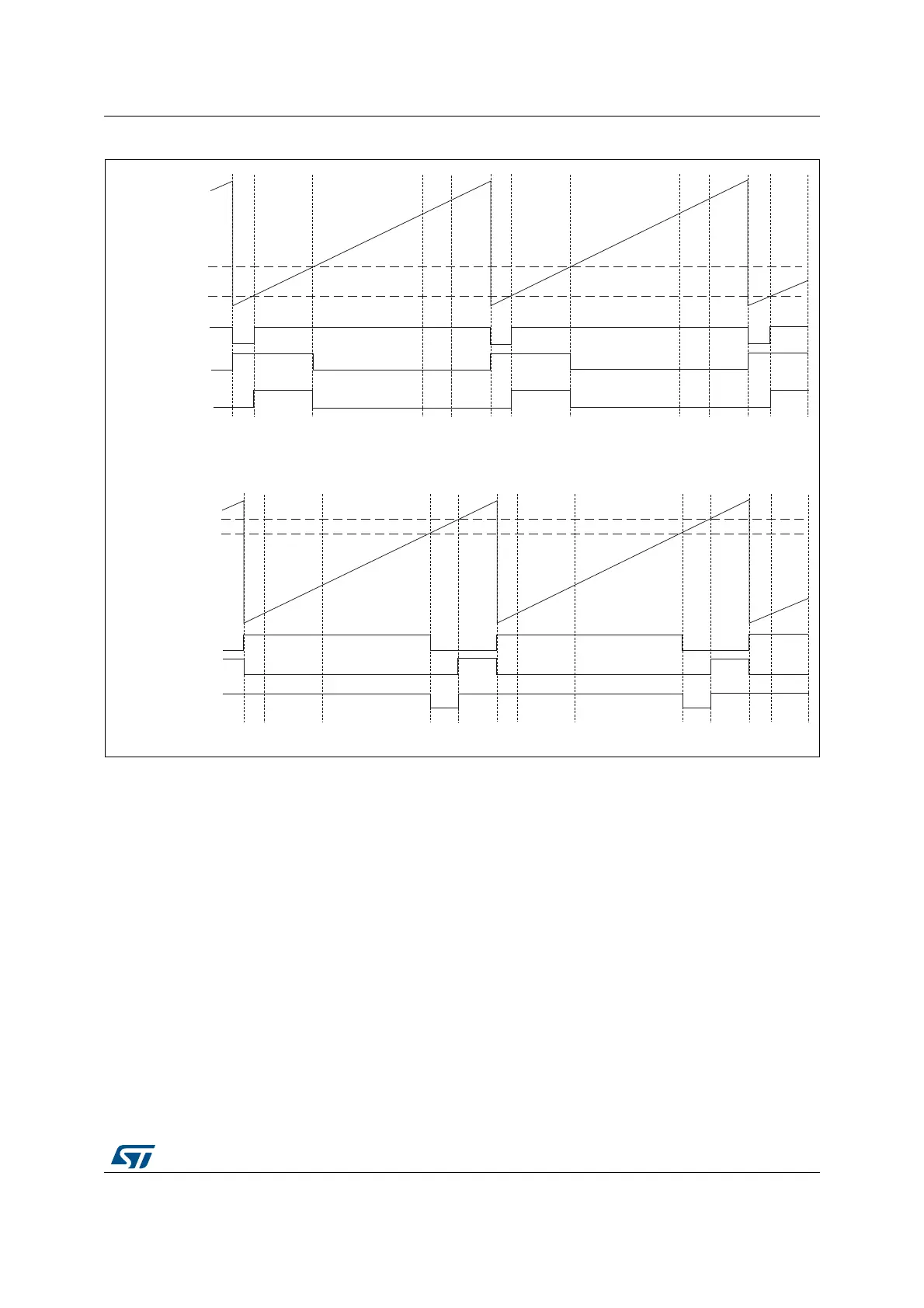
Figure 464. Combined PWM mode on channel 1 and 2
30.4.14 Complementary outputs and dead-time insertion
The TIM15/TIM16/TIM17 general-purpose timers can output one complementary signal and
manage the switching-off and switching-on of the outputs.
This time is generally known as dead-time and it has to be adjusted depending on the
devices that are connected to the outputs and their characteristics (intrinsic delays of level-
shifters, delays due to power switches...)
The polarity of the outputs (main output tim_ocx or complementary tim_ocxn) can be
selected independently for each output. This is done by writing to the CCxP and CCxNP bits
in the TIMx_CCER register.
The complementary signals tim_ocx and tim_ocxn are activated by a combination of several
control bits: the CCxE and CCxNE bits in the TIMx_CCER register and the MOE, OISx,
OISxN, OSSI and OSSR bits in the TIMx_BDTR and TIMx_CR2 registers. Refer to
Table 301: Output control bits for complementary tim_oc1 and tim_oc1n channels with
break feature (TIM16/TIM17) on page 1431 for more details. In particular, the dead-time is
activated when switching to the idle state (MOE falling down to 0).
MSv62330V1
tim_oc1ref
tim_oc2ref
tim_oc1refc
tim_oc1refc = tim_oc1ref AND tim_oc2ref
CCR1
CCR2
tim_oc1ref
tim_oc2ref
tim_oc1refc
tim1_oc1refc = tim1_oc1ref OR tim1_oc2ref
CCR1
CCR2
 Loading...


