RM0440 Rev 4 1365/2126
RM0440 General-purpose timers (TIM15/TIM16/TIM17)
1445
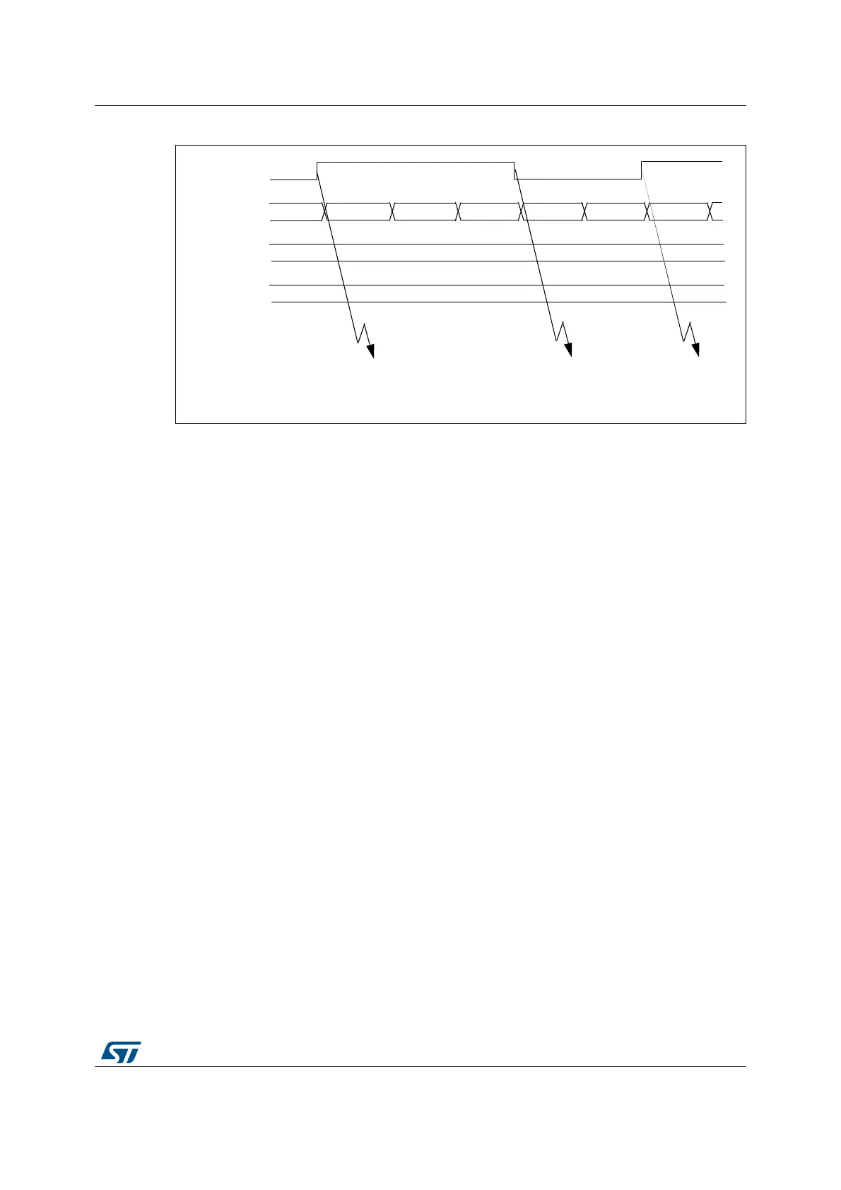
Figure 457. PWM input mode timing
1. The PWM input mode can be used only with the TIMx_CH1/TIMx_CH2 signals due to the fact that only
tim_ti1fp1 and tim_ti2fp2 are connected to the slave mode controller.
30.4.10 Forced output mode
In output mode (CCxS bits = 00 in the TIMx_CCMRx register), each output compare signal
(tim_ocxref and then tim_ocx/tim_ocxn) can be forced to active or inactive level directly by
software, independently of any comparison between the output compare register and the
counter.
To force an output compare signal (tim_ocxref/tim_ocx) to its active level, one just needs to
write 101 in the OCxM bits in the corresponding TIMx_CCMRx register. Thus tim_ocxref is
forced high (tim_ocxref is always active high) and tim_ocx get opposite value to CCxP
polarity bit.
For example: CCxP=0 (tim_ocx active high) => tim_ocx is forced to high level.
The tim_ocxref signal can be forced low by writing the OCxM bits to 100 in the
TIMx_CCMRx register.
Anyway, the comparison between the TIMx_CCRx shadow register and the counter is still
performed and allows the flag to be set. Interrupt and DMA requests can be sent
accordingly. This is described in the output compare mode section below.
30.4.11 Output compare mode
This function is used to control an output waveform or indicating when a period of time has
elapsed.
When a match is found between the capture/compare register and the counter, the output
compare function:
• Assigns the corresponding output pin to a programmable value defined by the output
compare mode (OCxM bits in the TIMx_CCMRx register) and the output polarity (CCxP
MSv62325V1
tim_ti1
TIMx_CNT
TIMx_CCR1
TIMx_CCR2
IC1 capture
IC2 capture
reset counter
IC2 capture
pulse width
measurement
IC1 capture
pulse width
measurement
0004 0000 0001 0002 0003 0004 0000
0004
0002
 Loading...


