RM0440 Rev 4 605/2126
RM0440 Analog-to-digital converters (ADC)
724
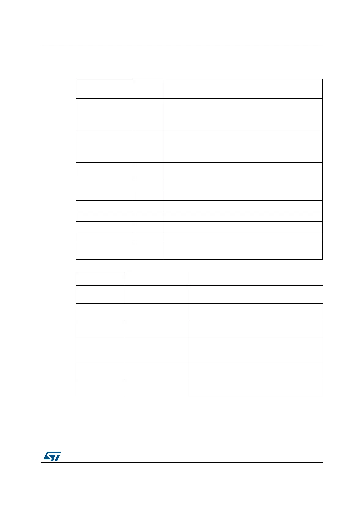
21.4.2 ADC pins and internal signals
Table 159. ADC internal input/output signals
Internal signal name
Signal
type
Description
adc_ext_trg[31:0] Inputs
Up to 32 external trigger inputs for the regular conversions (can
be connected to on-chip timers).
These inputs are shared between the ADC master and the ADC
slave.
adc_jext_trg[31:0] Inputs
Up to 31 external trigger inputs for the injected conversions (can
be connected to on-chip timers).
These inputs are shared between the ADC master and the ADC
slave.
adc_awdx_out Output
Internal analog watchdog output signal connected to on-chip
timers. (x = Analog watchdog number 1,2,3)
adc_ker_ck Output ADC kernel clock
adc_hclk Input ADC peripheral clock
adc_it Output ADC interrupt
adc_dma Output ADC DMA request
V
TS
Input Output voltage from internal temperature sensor
V
REFINT
Input Output voltage from internal reference voltage
V
BAT
Input
supply
External battery voltage supply
Table 160. ADC input/output pins
Pin name Signal type Comments
VREF+
Input, analog reference
positive
The higher/positive reference voltage for the ADC,
1.62 V ≤ V
REF+
≤ V
DDA
VDDA Input, analog supply
Analog power supply equal V
DDA
:
1.62 V ≤ V
DDA
≤ 3.6 V
VREF−
Input, analog reference
negative
The lower/negative reference voltage for the ADC.
V
REF−
is internally connected to V
SSA
VSSA
Input, analog supply
ground
Ground for analog power supply. On device package
which do not have a dedicated V
SSA
pin, V
SSA
is
internally connected to V
SS
.
V
INP
i
Positive analog input
channels for each ADC
Connected either to ADCx_INPi external channels or
to internal channels.
V
INN
i
Negative analog input
channels for each ADC
Connected either to V
REF−
or to external channels:
ADCx_INNi and ADCx_INP[i+1].
 Loading...


