Digital-to-analog converter (DAC) RM0440
744/2126 RM0440 Rev 4
Example of the sample and refresh time calculation with output buffer on
The values used in the example below are provided as indication only. Please refer to the
product datasheet for product data.
C
SH
= 100 nF
V
DDA
= 3.0 V
Sampling phase:
t
SAMP
= 7 μs + (10 * 2000 * 100 * 10
-9
) = 2.007 ms
(where R
BON
= 2 kΩ)
Refresh phase:
t
REFRESH
= 7 μs + (2000 * 100 * 10
-9
) * ln(2*10) = 606.1 μs
(where N
LSB
= 10 (10 LSB drop during the hold phase)
Hold phase:
D
v
= i
leak
* t
hold
/ C
SH
= 0.0073 V (10 LSB of 12bit at 3 V)
i
leak
= 150 nA (worst case on the IO leakage on all the temperature range)
t
hold
= 0.0073 * 100 * 10
-9
/ (150 * 10
-9
) = 4.867 ms
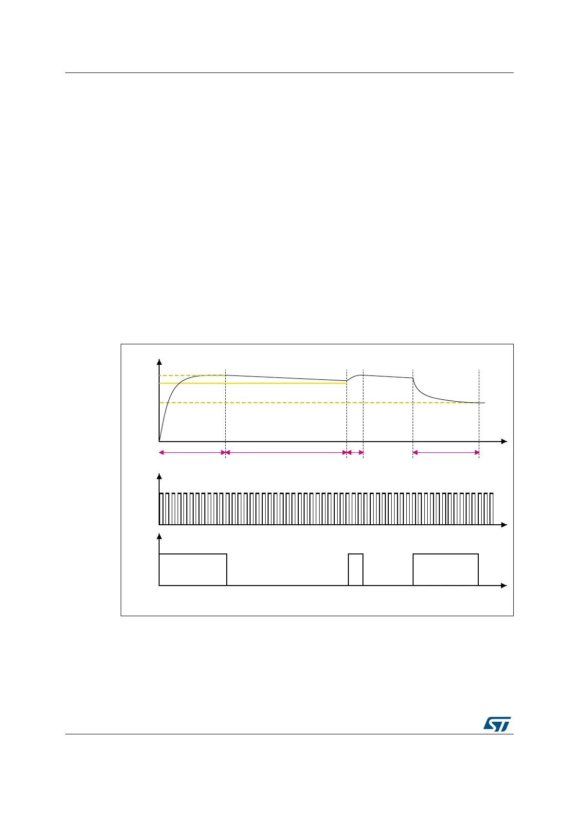
Figure 167. DAC Sample and hold mode phase diagram
Like in Normal mode, the Sample and hold mode has different configurations.
To enable the output buffer, MODEx[2:0] bits in DAC_MCR register must be set to:
• 100: DAC is connected to the external pin
• 101: DAC is connected to external pin and to on chip peripherals
MSv45340V3
dac_hold
_ck
DAC
ON ONON
t
t
V
1
V
2
Sampling phase Hold phase
Refresh
phase
Sampling phase
V
d