RM0440 Rev 4 269/2126
RM0440 Power control (PWR)
271
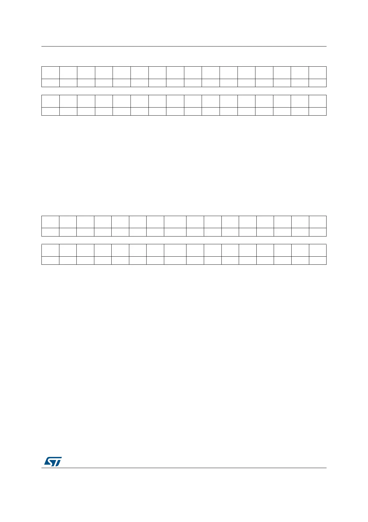
6.4.22 Power control register (PWR_CR5)
Address offset: 0x80.
Reset value: 0x0000 0100. This register is reset only by power on reset.
31 30 29 28 27 26 25 24 23 22 21 20 19 18 17 16
Res. Res. Res. Res. Res. Res. Res. Res. Res. Res. Res. Res. Res. Res. Res. Res.
1514131211109876543210
Res. Res. Res. Res. Res. PD10 PD9 PD8 PD7 PD6 PD5 PD4 PD3 PD2 PD1 PD0
rw rw rw rw rw rw rw rw rw rw rw
Bits 31:16
Reserved, must be kept at reset value.
Bits 15:0 PDy: Port G pull-down bit y (y=0..10)
When set, this bit activates the pull-down on PG[y] when APC bit is set in PWR_CR3 register.
31 30 29 28 27 26 25 24 23 22 21 20 19 18 17 16
Res. Res. Res. Res. Res. Res. Res. Res. Res. Res. Res. Res. Res. Res. Res. Res.
1514131211109 8 76543210
Res Res.Res.Res.Res.Res.Res.R1MODE Res. Res. Res. Res. Res. Res. Res. Res.
rw
Bits 31:9 Reserved, must be kept at reset value.
Bits 15:0 R1MODE: Main regular range 1 mode
This bit is only valid for the main regulator in range 1 and has no effect on range 2. It is
recommended to reset this bit when the system frequency is greater than 80 MHz. Refer to
Table 38: Range 1 boost mode configuration.
0: Main regulator in range 1 boost mode.
1: Main regulator in range 1 normal mode.
Bits 7:0 Reserved, must be kept at reset value.
 Loading...


