Embedded Flash memory (FLASH) for category 2 devices RM0440
190/2126 RM0440 Rev 4
5.3.2 Error code correction (ECC)
Data in Flash memory are 72-bits words: 8 bits are added per double word (64 bits). The
ECC mechanism supports:
• One error detection and correction
• Two errors detection
When one error is detected and corrected, the flag ECCC (ECC correction) is set in Flash
ECC register (FLASH_ECCR). If ECCCIE is set, an interrupt is generated.
When two errors are detected, a flag ECCD (ECC detection) is set in FLASH_ECCR
register. In this case, a NMI is generated.
When an ECC error is detected, the address of the failing double word is saved in
ADDR_ECC[20:0] in the FLASH_ECCR register. ADDR_ECC[2:0] are always cleared.
When ECCC or ECCD is set, ADDR_ECC is not updated if a new ECC error occurs.
FLASH_ECCR is updated only when ECC flags are cleared.
Note: For a virgin data: 0xFF FFFF FFFF FFFF FFFF, one error is detected and corrected but two
errors detection is not supported.
When an ECC error is reported, a new read at the failing address may not generate an ECC
error if the data is still present in the current buffer, even if ECCC and ECCD are cleared.
5.3.3 Read access latency
To correctly read data from Flash memory, the number of wait states (LATENCY) must be
correctly programmed in the Flash access control register (FLASH_ACR) according to the
frequency of the CPU clock (HCLK) and the internal voltage range of the device V
CORE
.
Refer to Section 6.1.5: Dynamic voltage scaling management. Table 29 shows the
correspondence between wait states and CPU clock frequency.
After reset, the CPU clock frequency is 16 MHz and 1 wait state (WS) is configured in the
FLASH_ACR register.
When changing the CPU frequency, the following software sequences must be applied in
order to tune the number of wait states needed to access the Flash memory:
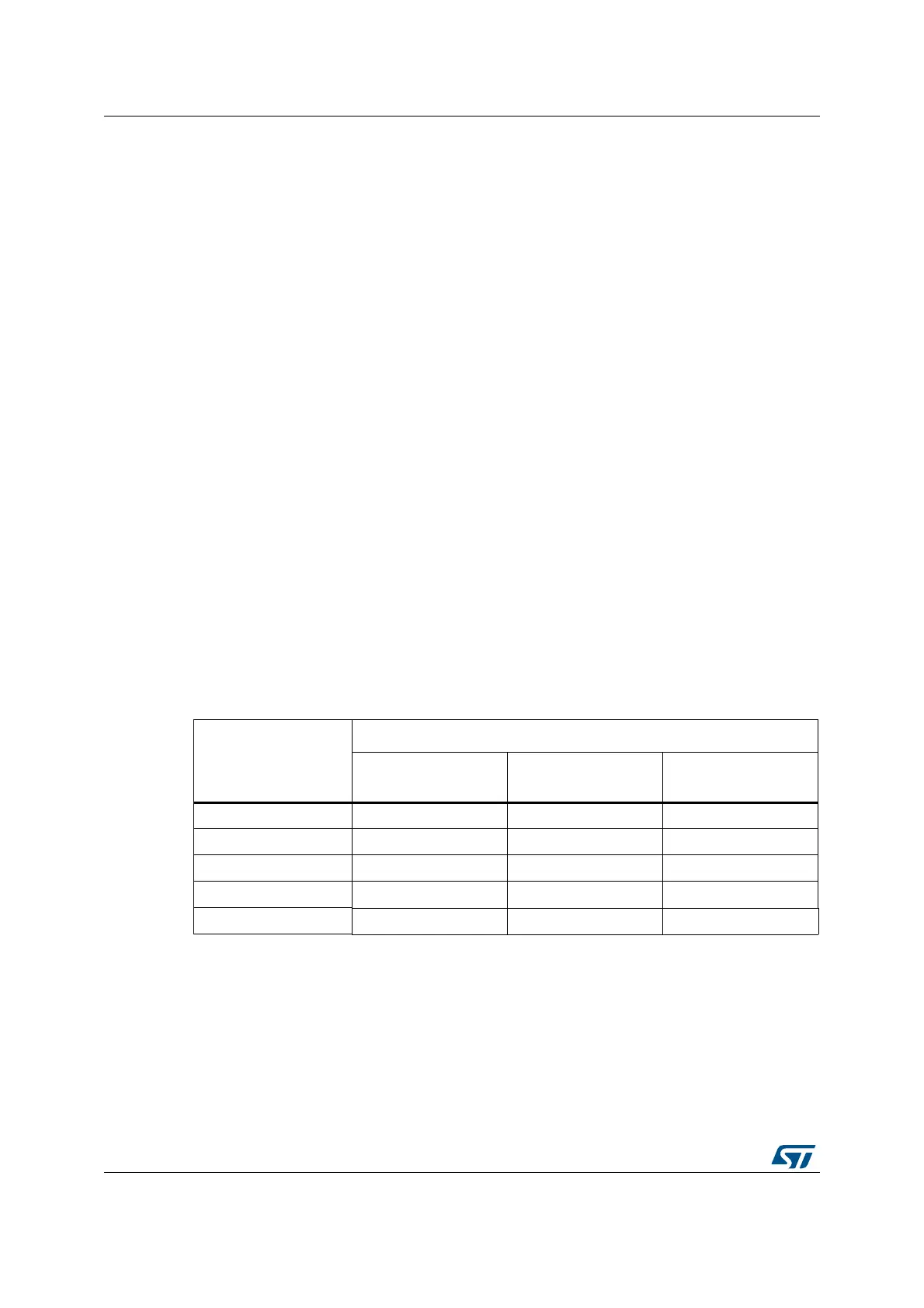
Table 29. Number of wait states according to CPU clock (HCLK) frequency
Wait states (WS)
(LATENCY)
HCLK (MHz)
V
CORE
Range 1
boost mode
V
CORE
Range 1
normal mode
V
CORE
Range 2
0 WS (1 CPU cycles) ≤ 34 ≤ 30 ≤ 12
1 WS (2 CPU cycles) ≤ 68 ≤ 60 ≤ 24
2 WS (3 CPU cycles) ≤ 102 ≤ 90 ≤ 26
3 WS (4 CPU cycles) ≤ 136 ≤ 120 -
4 WS (5 CPU cycles) ≤ 170 ≤ 150 -