RM0440 Rev 4 1447/2126
RM0440 Basic timers (TIM6/TIM7)
1463
31.3 TIM6/TIM7 functional description
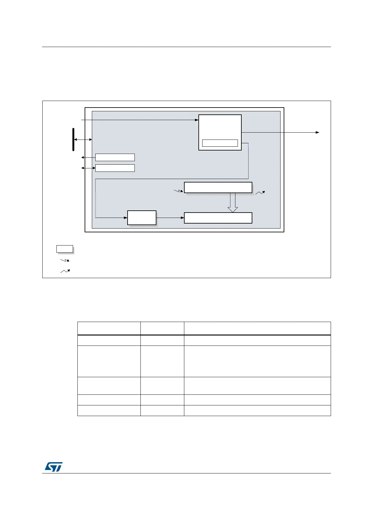
31.3.1 TIM6/TIM7 block diagram
Figure 479. Basic timer block diagram
31.3.2 TIM6/TIM7 internal signals
The table in this section summarizes the TIM inputs and outputs.
MSv62381V1
CNT counter
tim_ker_ck
Auto-reload register
+
tim_psc_ck
tim_cnt_ck
Stop, clear or up
Update
UEV
Notes:
Preload registers transferred to active registers on U event according to control bit
Event
Interrupt & DMA
Enable
Count
tim_pck
tim_trgo
Trigger controller
Control
Reg
PSC
prescaler
Auto-reload register
32-bit
APB bus
DMA interface
IRQ interface
tim_upd_dma
tim_upd_it
Table 303. TIM internal input/output signals
Internal signal name Signal type Description
tim_pclk Input Timer APB clock
tim_ker_ck Input
Timer kernel clock. This clock must be synchronous with
tim_pclk (derived from the same source). The clock ratio
tim_ker_ck/tim_pclk must be an integer:1, 2, 3,..., 16
(maximum value)
tim_trgo Output
Internal trigger output. This trigger can trigger other on-
chip peripherals (DAC).
tim_upd_it Output Timer update event interrupt
tim_upd_dma Output Timer update dma request
 Loading...


