RM0440 Rev 4 2083/2126
RM0440 Debug support (DBG)
2112
47.4.1 SWJ debug port pins
Five pins are used as outputs from the STM32G4 Series for the SWJ-DP as alternate
functions of general-purpose I/Os. These pins are available on all packages.
47.4.2 Flexible SWJ-DP pin assignment
After RESET (SYSRESETn or PORESETn), all five pins used for the SWJ-DP are assigned
as dedicated pins immediately usable by the debugger host (note that the trace outputs are
not assigned except if explicitly programmed by the debugger host).
However, the STM32G4 Series MCUs offer the possibility of disabling some or all of the
SWJ-DP ports, and therefore the possibility of releasing (in gray in the table below) the
associated pins for general-purpose I/O (GPIO) usage, except for NJTRST that can be left
disconnected but cannot be used as general purpose GPIO without loosing debugger
connection. For more details on how to disable SWJ-DP port pins, please refer to
Section 9.3.2: I/O pin alternate function multiplexer and mapping.
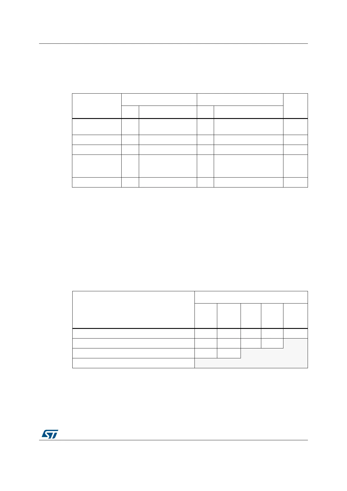
Table 430. SWJ debug port pins
SWJ-DP pin name
JTAG debug port SW debug port Pin
assign
ment
Type Description Type Debug assignment
JTMS/SWDIO I
JTAG Test Mode
Selection
IO
Serial Wire Data
Input/Output
PA13
JTCK/SWCLK I JTAG Test Clock I Serial Wire Clock PA14
JTDI I JTAG Test Data Input - - PA15
JTDO/TRACESWO O JTAG Test Data Output -
TRACESWO if
asynchronous trace is
enabled
PB3
NJTRST I JTAG Test nReset - - PB4
Table 431. Flexible SWJ-DP pin assignment
Available debug ports
SWJ IO pin assigned
PA13 /
JTMS/
SWDIO
PA14 /
JTCK/
SWCLK
PA15 /
JTDI
PB3 /
JTDO
PB4/
NJTRST
Full SWJ (JTAG-DP + SW-DP) - Reset State X X X X X
Full SWJ (JTAG-DP + SW-DP) but without NJTRST X X X X
JTAG-DP disabled and SW-DP enabled X X
JTAG-DP disabled and SW-DP disabled Released
 Loading...


