High-resolution timer (HRTIM) RM0440
848/2126 RM0440 Rev 4
27.3.2 HRTIM pins and internal signals
The tables in this section summarize the HRTIM inputs and outputs, both on-chip and off-
chip.
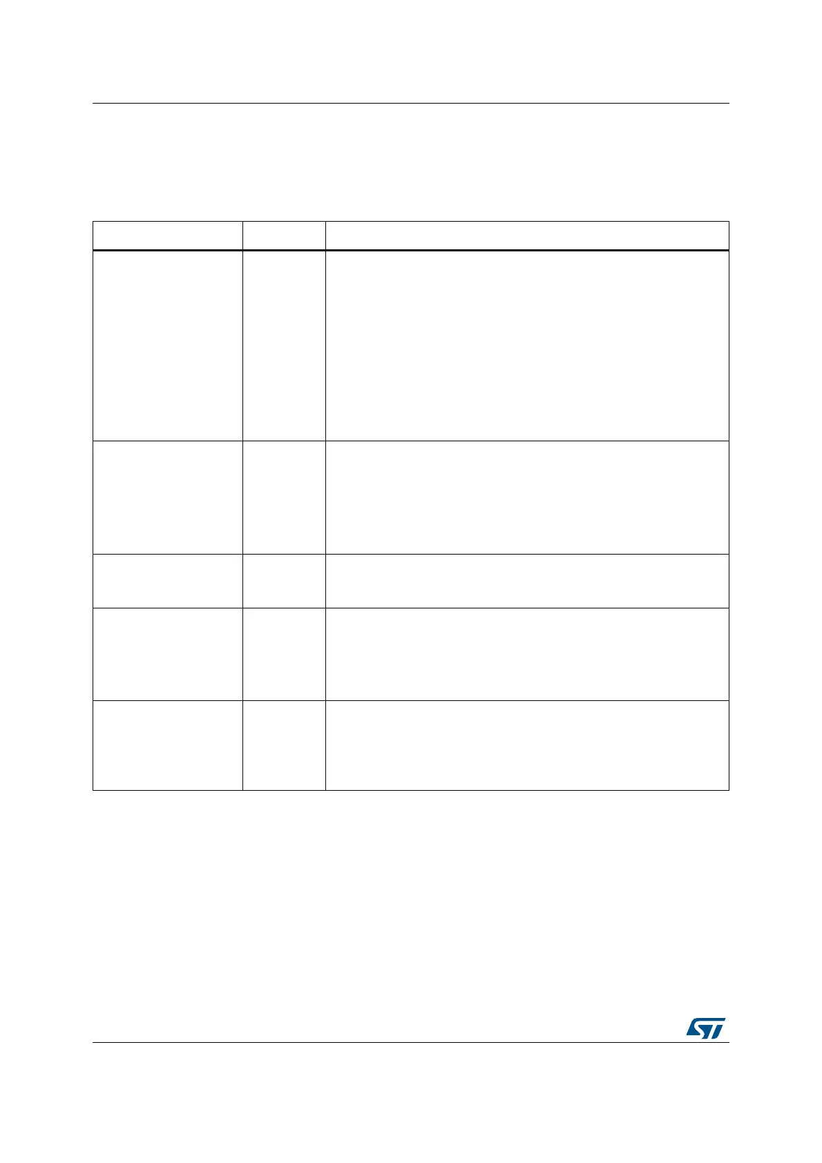
Table 207. HRTIM inputs/outputs summary
Signal name Signal type Description
HRTIM_CHA1,
HRTIM_CHA2,
HRTIM_CHB1,
HRTIM_CHB2,
HRTIM_CHC1,
HRTIM_CHC2,
HRTIM_CHD1,
HRTIM_CHD2,
HRTIM_CHE1,
HRTIM_CHE2,
HRTIM_CHF1,
HRTIM_CHF2
Outputs
Main HRTIM timer outputs. They can be coupled by pairs (HRTIM_CHx1
& HRTIM_CHx2) with deadtime insertion or work independently.
hrtim_in_flt1[4:1]
hrtim_in_flt2[4:1]
hrtim_in_flt3[4:1]
hrtim_in_flt4[4:1]
hrtim_in_flt5[4:1]
hrtim_in_flt6[4:1]
Digital input
Fault inputs: immediately disable the HRTIM outputs when asserted (12
on-chip inputs and 6 off-chip HRTIM_FLTx inputs).
hrtim_sys_flt Digital input
System fault gathering MCU internal fault events (clock security system,
SRAM parity error, Cortex
®
-M4 with FPU lockup (HardFault), PVD
output.
hrtim_in_sync[3:1] Digital Input
Synchronization inputs to synchronize the whole HRTIM with other
internal or external timer resources:
hrtim_in_sync1: Reserved
hrtim_in_sync2: the source is the TIM1_TRGO output
hrtim_in_sync3: the source is HRTIM_SCIN input pins
hrtim_out_sync[2:1] Digital output
The purpose of this output is to cascade or synchronize several HRTIM
instances, either on-chip or off-chip:
hrtim_out_sync1: Reserved
hrtim_out_sync2: the destination is an off-chip HRTIM or peripheral (via
HRTIM_SCOUT output pins)
 Loading...


