RM0440 Rev 4 737/2126
RM0440 Digital-to-analog converter (DAC)
773
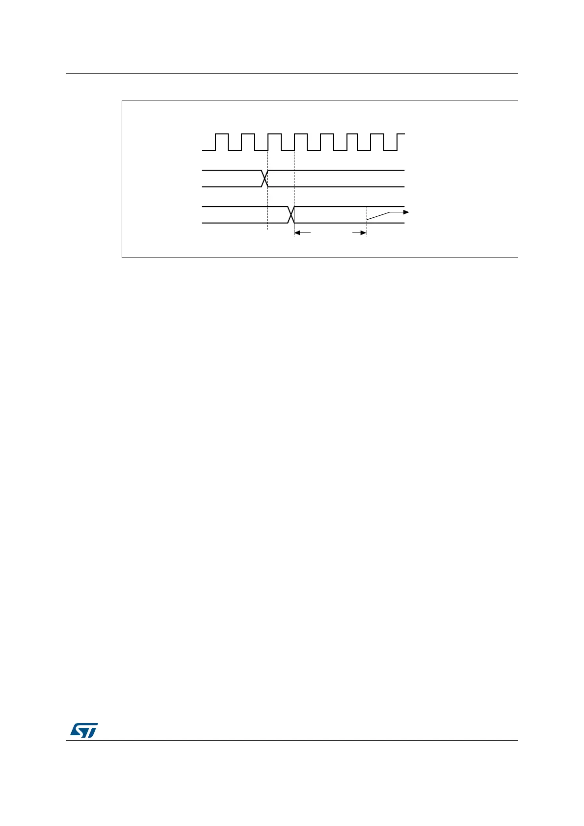
Figure 159. Timing diagram for conversion with trigger disabled TEN = 0
22.4.6 DAC output voltage
Digital inputs are converted to output voltages on a linear conversion between 0 and V
REF+
.
The analog output voltages on each DAC channel pin are determined by the following
equation:
22.4.7 DAC trigger selection
If the TENx control bit is set, the conversion can then be triggered by an external event (timer
counter, external interrupt line). The TSELx[3:0] control bits determine which out of 16 pos-
sible events triggers the conversion as shown in TSELx[3:0] bits of the DAC_CR register.
These events can be either the software trigger or hardware triggers. Refer to the intercon-
nection table in Section 22.4.2: DAC pins and internal signals.
Each time a DAC interface detects a rising edge on the selected trigger source (refer to the
table below), the last data stored into the DAC_DHRx register are transferred into the
DAC_DORx register. The DAC_DORx register is updated three dac_hclk cycles after the
trigger occurs.
If the software trigger is selected, the conversion starts once the SWTRIG bit is set.
SWTRIG is reset by hardware once the DAC_DORx register has been loaded with the
DAC_DHRx register contents.
The reset trigger selection and the increment trigger selection of the sawtooth generation
are performed through STRSTTRIGSELx and STINCTRIGSELx control bits, respectively.
STRSTTRIGSELx mapping is similar to TSELx. Refer to Section 22.4.2: DAC pins and
internal signals for TSELx, STRSTTRIGSELx, and STINCTRIGSELx mappings.
Note: TSELx[3:0] bit cannot be changed when the ENx bit is set.
When software trigger is selected, the transfer from the DAC_DHRx register to the
DAC_DORx register takes only one dac_hclk clock cycle.
MSv45319V2
Bus clock
0x1AC
0x1AC
tSETTLING
DHR
DOR
Output voltage available on
DAC_OUT pin
DACoutput V
REF
DOR
4096
--------------
×=
 Loading...


