Serial audio interface (SAI) RM0440
1794/2126 RM0440 Rev 4
40.3 SAI functional description
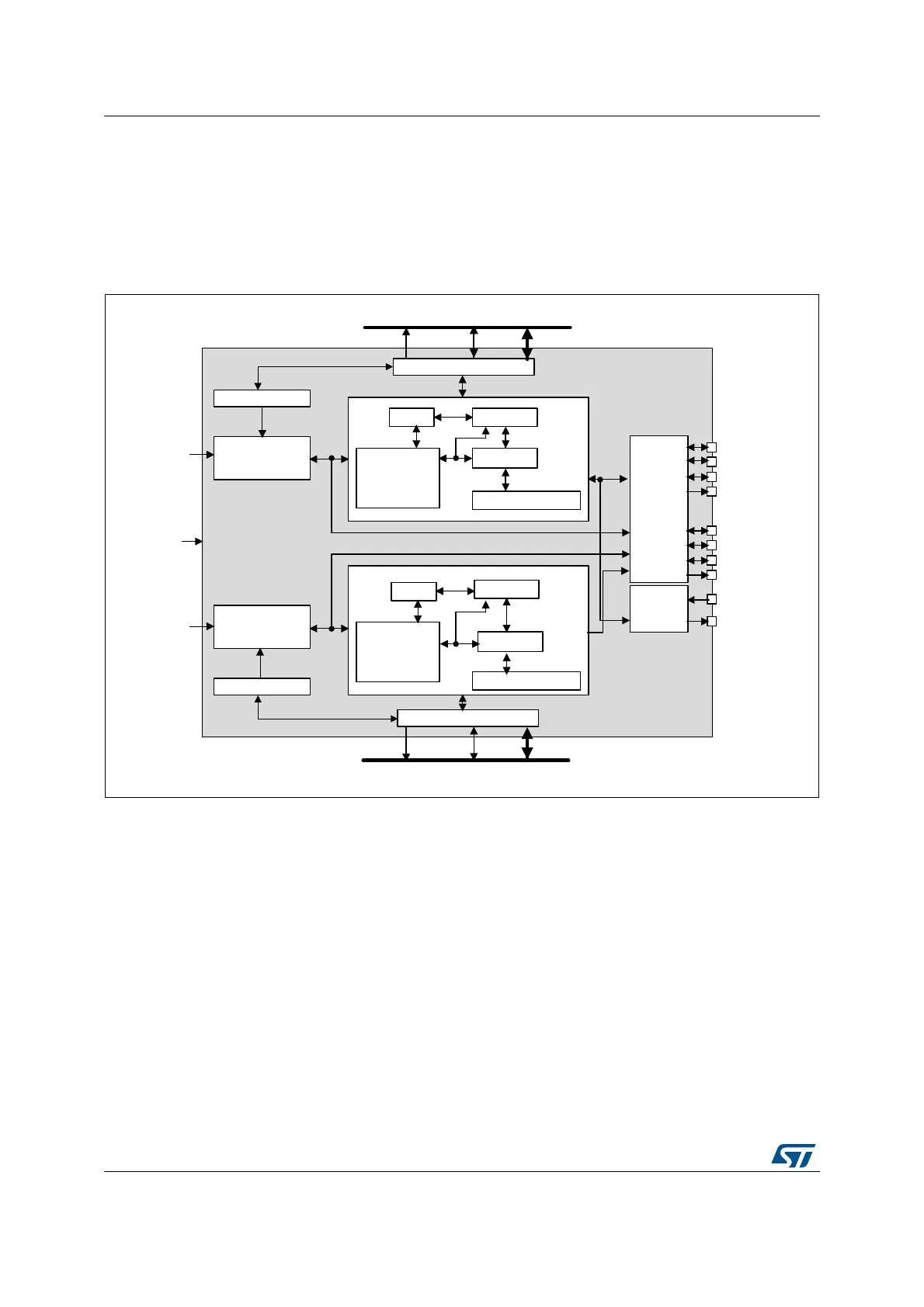
40.3.1 SAI block diagram
Figure 608 shows the SAI block diagram while Table 362 and Table 363 list SAI internal and
external signals.
Figure 608. SAI functional block diagram
The SAI is mainly composed of two audio subblocks with their own clock generator. Each
audio block integrates a 32-bit shift register controlled by their own functional state machine.
Data are stored or read from the dedicated FIFO. FIFO may be accessed by the CPU, or by
DMA in order to leave the CPU free during the communication. Each audio block is
independent. They can be synchronous with each other.
An I/O line controller manages a set of 4 dedicated pins (SD, SCK, FS, MCLK) for a given
audio block in the SAI. Some of these pins can be shared if the two subblocks are declared
as synchronous to leave some free to be used as general purpose I/Os. The MCLK pin can
be output, or not, depending on the application, the decoder requirement and whether the
audio block is configured as the master.
If one SAI is configured to operate synchronously with another one, even more I/Os can be
freed (except for pins SD_x).
The functional state machine can be configured to address a wide range of audio protocols.
Some registers are present to set-up the desired protocols (audio frame waveform
generator).
MSv62452V1
D[4:1]
CK[4:1]
FIFO FIFO ctrl
Configuration
and status
registers
FSM
32-bit shift register
Audio block A
FIFO
FIFO ctrl
Configuration
and status
registers
FSM
32-bit shift register
Audio block B
Clock generator
Audio block A
SAI_ACR1
SAI_BCR1
Clock generator
Audio block B
APB Interface
APB Interface
IO Line Management
SAI
FS_A
SD_A
SCK_A
MCLK_A
FS_B
SD_B
SCK_B
MCLK_B
PDM_IF
32-bit APB bus
32-bit APB bus
sai_a_gbl_it
sai_b_gbl_it
sai_b_dma
sai_a_dma
sai_a_
ker_ck
sai_b_
ker_ck
sai_pclk
 Loading...


