Reset and clock control (RCC) RM0440
314/2126 RM0440 Rev 4
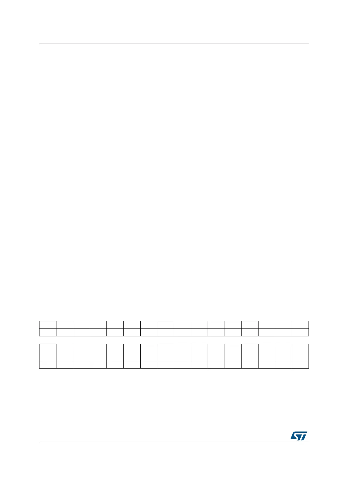
7.4.18 APB1 peripheral clock enable register 2 (RCC_APB1ENR2)
Address offset: 0x5C
Reset value: 0x0000 0000
Access: no wait state, word, half-word and byte access
Note: When the peripheral clock is not active, the peripheral registers read or write access is not
supported.
Bit 5 TIM7EN: TIM7 timer clock enable
Set and cleared by software.
0: TIM7 clock disabled
1: TIM7 clock enabled
Bit 4 TIM6EN: TIM6 timer clock enable
Set and cleared by software.
0: TIM6 clock disabled
1: TIM6 clock enabled
Bit 3 TIM5EN: TIM5 timer clock enable
Set and cleared by software.
0: TIM5 clock disabled
1: TIM5 clock enabled
Bit 2 TIM4EN: TIM4 timer clock enable
Set and cleared by software.
0: TIM4 clock disabled
1: TIM4 clock enabled
Bit 1 TIM3EN: TIM3 timer clock enable
Set and cleared by software.
0: TIM3 clock disabled
1: TIM3 clock enabled
Bit 0 TIM2EN: TIM2 timer clock enable
Set and cleared by software.
0: TIM2 clock disabled
1: TIM2 clock enabled
31 30 29 28 27 26 25 24 23 22 21 20 19 18 17 16
Res. Res. Res. Res. Res. Res. Res. Res. Res. Res. Res. Res. Res. Res. Res. Res.
1514131211109876543210
Res. Res. Res. Res. Res. Res. Res.
UCPD1
EN
Res. Res. Res. Res. Res. Res. I2C4EN
LP
UART1
EN
rw rw rw
 Loading...


