Analog-to-digital converters (ADC) RM0440
718/2126 RM0440 Rev 4
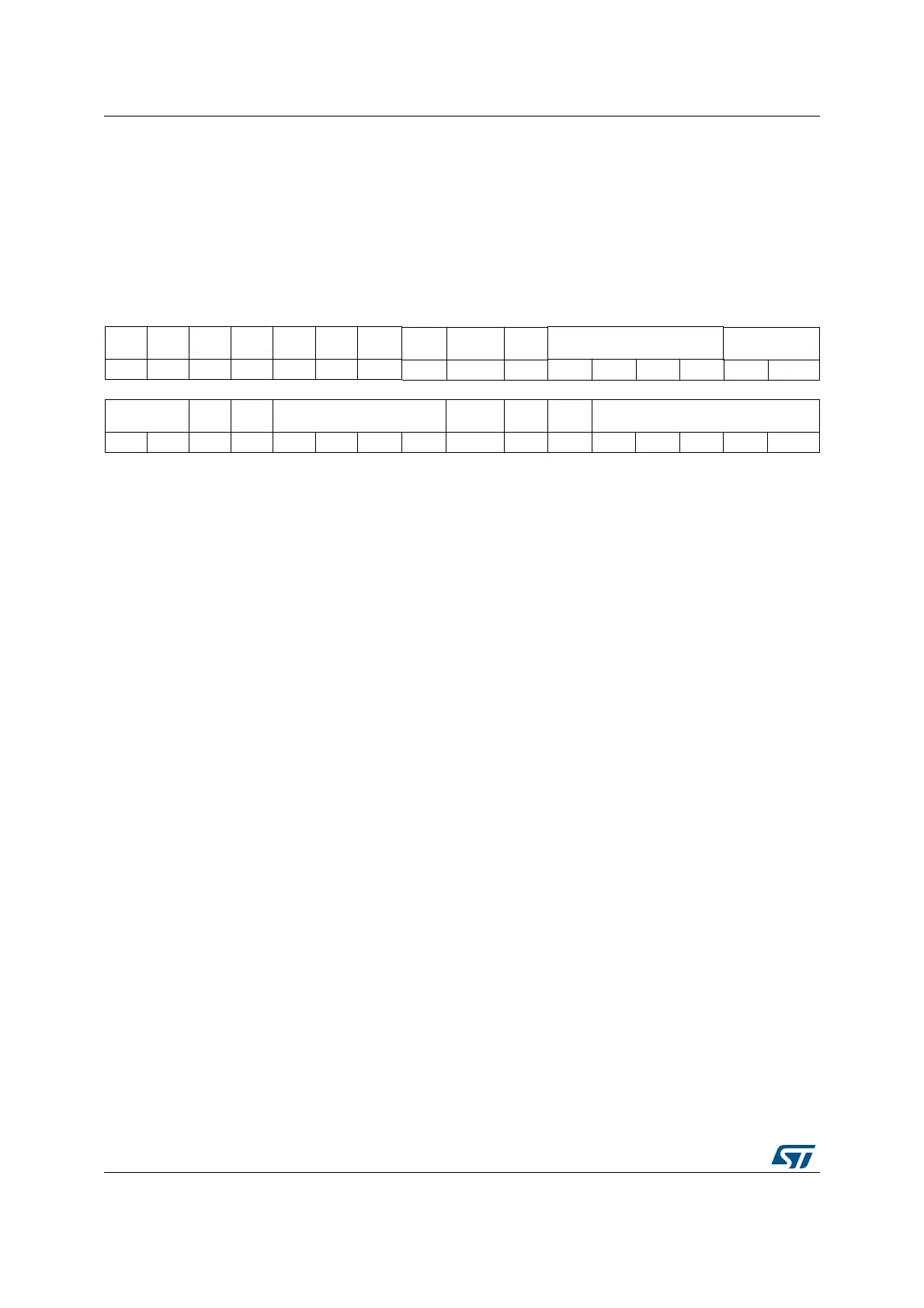
21.7.2 ADCx common control register (ADCx_CCR) (x=12 or 345)
Address offset: 0x08 (this offset address is relative to the master ADC base address +
0x300)
Reset value: 0x0000 0000
One interface controls ADC1 and ADC2, while the other interface controls ADC3, ADC4 and
ADC5.
31 30 29 28 27 26 25 24 23 22 21 20 19 18 17 16
Res. Res. Res. Res. Res. Res. Res.
VBATS
EL
VSENSES
EL
VREF
EN
PRESC[3:0] CKMODE[1:0]
rw rw rw rw rw rw rw rw rw
15141312111098 7 654321 0
MDMA[1:0]
DMA
CFG
Res. DELAY[3:0] Res. Res. Res. DUAL[4:0]
rw rw rw rw rw rw rw rw rw rw rw rw
Bits 31:25 Reserved, must be kept at reset value.
Bit 24 VBATSEL: VBAT selection
This bit is set and cleared by software to control VBAT.
0: V
BAT
channel disabled.
1: V
BAT
channel enabled
Bit 23 VSENSESEL: V
TS
selection
This bit is set and cleared by software to control V
TS
.
0: Temperature sensor channel disabled
1: Temperature sensor channel enabled
Bit 22 VREFEN: V
REFINT
enable
This bit is set and cleared by software to enable/disable the V
REFINT
channel.
0: V
REFINT
channel disabled
1: V
REFINT
channel enabled
Bits 21:18 PRESC[3:0]: ADC prescaler
These bits are set and cleared by software to select the frequency of the clock to the ADC.
The clock is common for all the ADCs.
0000: input ADC clock not divided
0001: input ADC clock divided by 2
0010: input ADC clock divided by 4
0011: input ADC clock divided by 6
0100: input ADC clock divided by 8
0101: input ADC clock divided by 10
0110: input ADC clock divided by 12
0111: input ADC clock divided by 16
1000: input ADC clock divided by 32
1001: input ADC clock divided by 64
1010: input ADC clock divided by 128
1011: input ADC clock divided by 256
other: reserved
Note: The software is allowed to write these bits only when the ADC is disabled (ADCAL=0,
JADSTART=0, ADSTART=0, ADSTP=0, ADDIS=0 and ADEN=0). The ADC prescaler
value is applied only when CKMODE[1:0] = 0b00.
 Loading...


