RM0440 Rev 4 1391/2126
RM0440 General-purpose timers (TIM15/TIM16/TIM17)
1445
30.7 TIM15 registers
Refer to Section 1.2 for a list of abbreviations used in register descriptions.
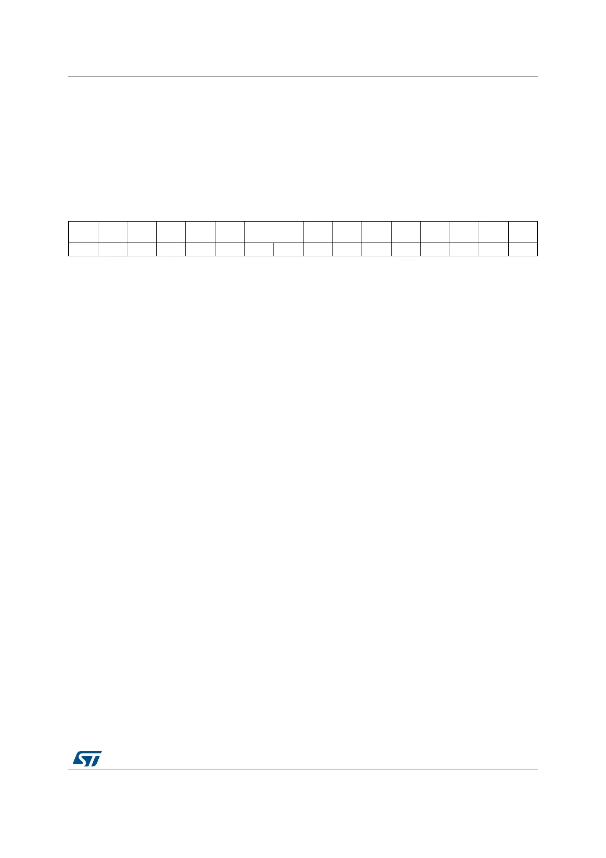
30.7.1 TIM15 control register 1 (TIM15_CR1)
Address offset: 0x00
Reset value: 0x0000
1514131211109876543210
Res. Res. Res.
DITH
EN
UIFRE
MAP
Res. CKD[1:0] ARPE Res. Res. Res. OPM URS UDIS CEN
rw rw rw rw rw rw rw rw rw
Bits 15:13 Reserved, must be kept at reset value.
Bit 12 DITHEN: Dithering enable
0: Dithering disabled
1: Dithering enabled
Note: The DITHEN bit can only be modified when CEN bit is reset.
Bit 11 UIFREMAP: UIF status bit remapping
0: No remapping. UIF status bit is not copied to TIM15_CNT register bit 31.
1: Remapping enabled. UIF status bit is copied to TIM15_CNT register bit 31.
Bit 10 Reserved, must be kept at reset value.
Bits 9:8 CKD[1:0]: Clock division
This bitfield indicates the division ratio between the timer clock (tim_ker_ck) frequency and
the dead-time and sampling clock (t
DTS
) used by the dead-time generators and the digital
filters (tim_tix)
00: t
DTS
= t
tim_ker_ck
01: t
DTS
= 2*t
tim_ker_ck
10: t
DTS
= 4*t
tim_ker_ck
11: Reserved
Bit 7 ARPE: Auto-reload preload enable
0: TIM15_ARR register is not buffered
1: TIM15_ARR register is buffered
Bits 6:4 Reserved, must be kept at reset value.
Bit 3 OPM: One-pulse mode
0: Counter is not stopped at update event
1: Counter stops counting at the next update event (clearing the bit CEN)
 Loading...


