RM0440 Rev 4 1413/2126
RM0440 General-purpose timers (TIM15/TIM16/TIM17)
1445
30.7.18 TIM15 input selection register (TIM15_TISEL)
Address offset: 0x5C
Reset value: 0x0000 0000
Bit 16 DTAE: Deadtime asymmetric enable
0:Deadtime on rising and falling edges are identical, and defined with DTG[7:0] register
1:Deadtime on rising edge is defined with DTG[7:0] register and deadtime on falling edge is
defined with DTGF[7:0] bits.
Note: This bit can not be modified as long as LOCK level 1, 2 or 3 has been programmed
(LOCK bits in TIM15_BDTR register).
Bits 15:8 Reserved, must be kept at reset value.
Bits 7:0 DTGF[7:0]: Dead-time falling edge generator setup
This bit-field defines the duration of the dead-time inserted between the complementary
outputs, on the falling edge.
DTGF[7:5]=0xx => DTF=DTGF[7:0]x t
dtg
with t
dtg
=t
DTS
.
DTGF[7:5]=10x => DTF=(64+DTGF[5:0])xt
dtg
with T
dtg
=2xt
DTS
.
DTGF[7:5]=110 => DTF=(32+DTGF[4:0])xt
dtg
with T
dtg
=8xt
DTS
.
DTGF[7:5]=111 => DTF=(32+DTGF[4:0])xt
dtg
with T
dtg
=16xt
DTS
.
Example if T
DTS
=125ns (8MHz), dead-time possible values are:
0 to 15875 ns by 125 ns steps,
16 us to 31750 ns by 250 ns steps,
32 us to 63us by 1 us steps,
64 us to 126 us by 2 us steps
Note: This bit-field can not be modified as long as LOCK level 1, 2 or 3 has been programmed
(LOCK bits in TIM15_BDTR register).
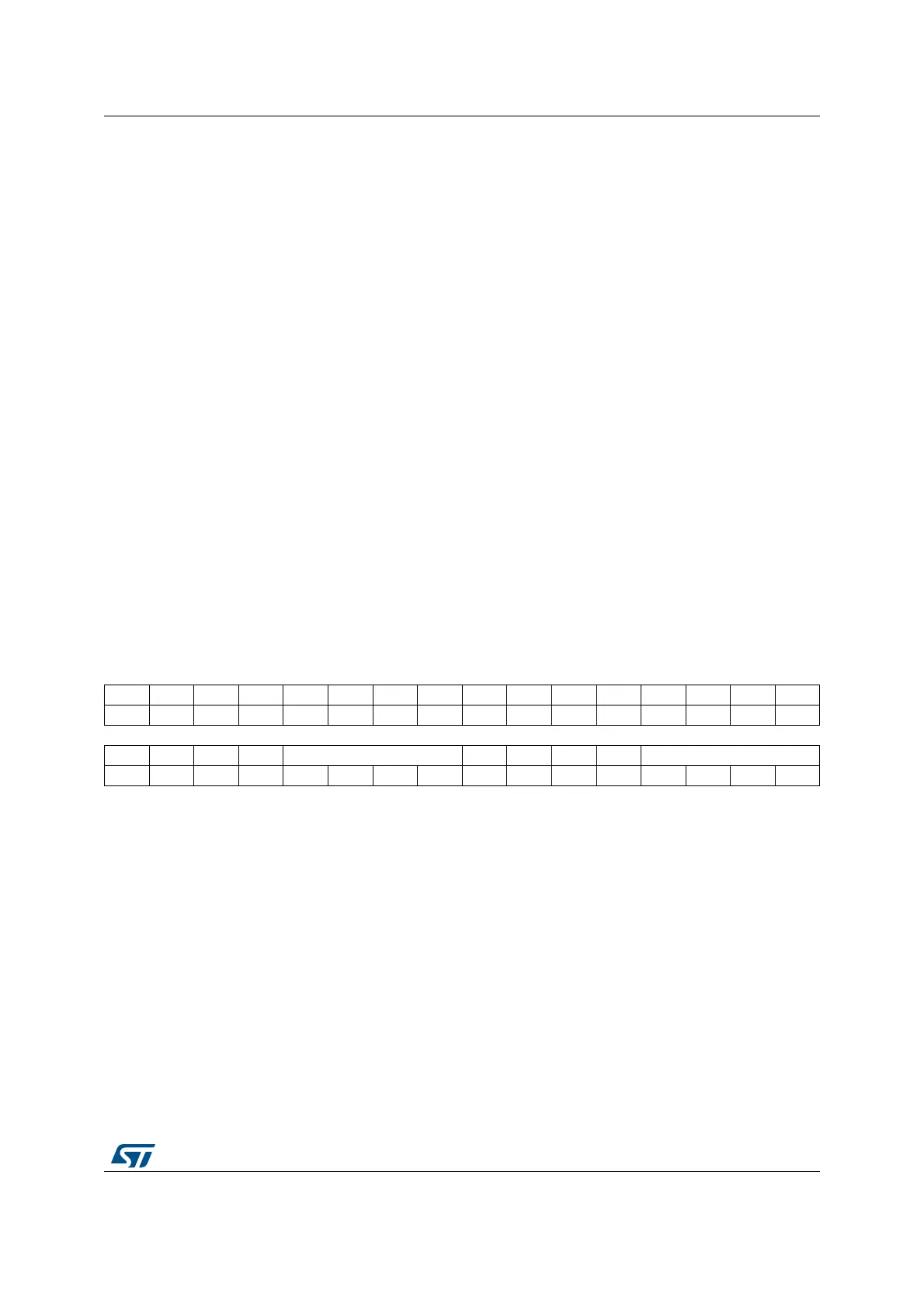
31 30 29 28 27 26 25 24 23 22 21 20 19 18 17 16
Res. Res. Res. Res. Res. Res. Res. Res. Res. Res. Res. Res. Res. Res. Res. Res.
1514131211109876543210
Res. Res. Res. Res. TI2SEL[3:0] Res. Res. Res. Res. TI1SEL[3:0]
rw rw rw rw rw rw rw rw
Bits 31:12 Reserved, must be kept at reset value.
Bits 11:8 TI2SEL[3:0]: selects tim_ti2_in[0..15] input
0000: TIM15_CH2 input (tim_ti2_in0)
0001: tim_ti2_in1
...
1111: tim_ti2_in15
Refer to Section 30.4.2: TIM15/TIM16/TIM17 pins and internal signals for interconnects list.
Bits 7:4 Reserved, must be kept at reset value.
Bits 3:0 TI1SEL[3:0]: selects tim_ti1_in[0..15] input
0000: TIM15_CH1 input (tim_ti1_in0)
0001: tim_ti1_in1
...
1111: tim_ti1_in15
Refer to Section 30.4.2: TIM15/TIM16/TIM17 pins and internal signals for interconnects list.
 Loading...


